-
-
November 16, 2023 at 6:53 am
-
November 18, 2023 at 12:51 am
Amrita Pati
Ansys EmployeeHi Mariah,
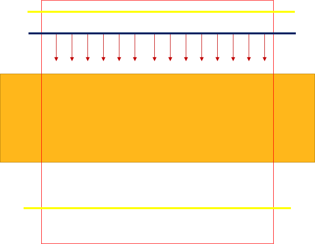
If you are simulating a cube (as opposed to a continuous layer), try to have a distance of lambda/2 between the cube and the PML boundaries. In the current configuration, I believe that, what is being calculated is the amount of absorption in a small cubical volume. But the structure itself extends through the PML, which is the default if the structure touches the inner PML boundaries. In other words, you are calculating the absorption in a cubical portion of a layer thats extending semi-infinitely in two directions. Which will be different than the absorption in an isolated cube. So, if you are trying to calculate the absorption in an isolated cube, I believe this example: Calculating absorbed optical power – Higher accuracy method with multiple materials will be very similar to your simulation.
Let me know if you have any questions.
Regards,
Amrita -
November 18, 2023 at 6:52 am
Mariah Ha
SubscriberWhat about using transmission and reflection monitors , and calculate the absorption asA=1-R-T as being used in the planar solar cell example? Does it work for this example?
-
November 21, 2023 at 7:46 pm
-
- The topic ‘low absoption of silicon at 850 nm FDTD’ is closed to new replies.


-
5664
-
1890
-
1419
-
1304
-
1021

© 2026 Copyright ANSYS, Inc. All rights reserved.


