TAGGED: antenna-design, ground, pcb, Port, sma
-
-
July 27, 2022 at 11:57 pm
Stefano R
SubscriberHello,
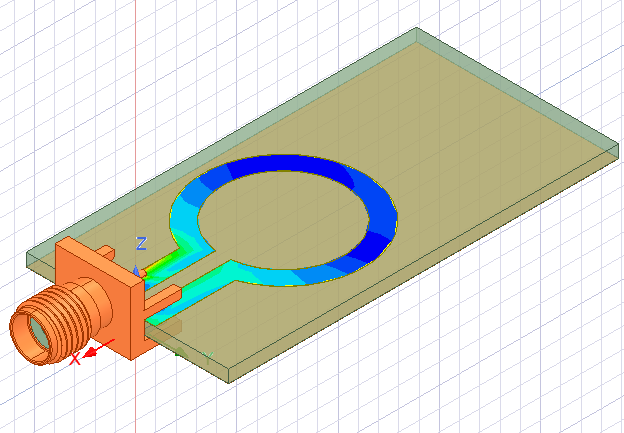
I have an SMA connector connected to a PCB with a trace in the shape of a loop antenna. The PCB has a ground plane on the back with a Perfect E condition. I connected the bottom side of the SMA to the ground plane using a Solder material block. I have a Lumped Port from the inner conductor to outer conductor of the SMA. I am not getting the results as in my real experiment, so I am wondering if its the way I defined the Port or Ground. Any help is appreciated. Thanks.
-
July 29, 2022 at 1:53 pm
Praneeth
Ansys EmployeeHello,
Please let us know how are you connecting the SMA connector pins to the loop antenna in the real experiment.
It looks like the simulation is not set up according to the real experiment. In general, the port exciation should be connected between the two opens ends of loop antenna. But as per your description it is not the case. Correct me if I am wrong.
If you are new to Ansys HFSS simulation, then you can connect the two open ends of the loop antenna with a rectangular sheet and assign lumped port instead of using a SMA connector.
All the very best,
Praneeth. -
July 29, 2022 at 4:49 pm
Stefano R
SubscriberPraneeth,
I have done simulations without the SMA using that port configuration you mentioned and it gives satisfying results. I wanted to take the model one step further by introducing the SMA connector. In the model I have the SMA touching the copper trace, but not sure if this is the best way to connect. Also, let me know if you think this path forward won't add much value to my results.
Thanks.
-
August 2, 2022 at 10:44 am
Praneeth
Ansys EmployeeHi,
Generally, users simulate their models with lumped or waveports available in the tool instead of simulating with the connectors as this saves their simulation resources. The response with these ports will be similar to that of the Connector ones.
You can simulate with the SMA connector if required. Try to conncet the connector like in the experiment. You can also use the inbuilt SMA connector under 3D components.
All the very best,
Praneeth. -
August 12, 2022 at 7:25 pm
Stefano R
SubscriberPraneeth,
How do you know the port response is similat to that of the Connectors? If this is the case, then it will save me some time and effort.
Also, does the size of the rectangular port connecting the open ends of the antenna matter much?
Thanks so much.
-
August 16, 2022 at 8:28 am
Praneeth
Ansys EmployeeGenerally, you would be using 50 ohms impedance connector for RF applications. Same can be achieved using the ports inside Ansys HFSS. These are provided for user convenience in simplifying the model. You can go through this Ansys Innovation Course for more details on the ports - Ansys HFSS Port Types - ANSYS Innovation Courses.
For the case of microstrip traces, there are specific guidelines when using a waveport. This is required to capture the fringing fields. Please go through "wave port size" section of the Ansys HFSS Help document.
All the very best,
Praneeth. -
August 18, 2022 at 8:09 pm
Stefano R
SubscriberPraneeth,
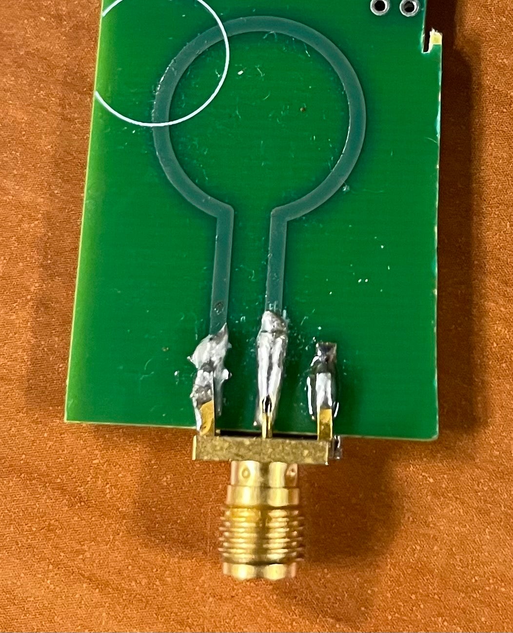
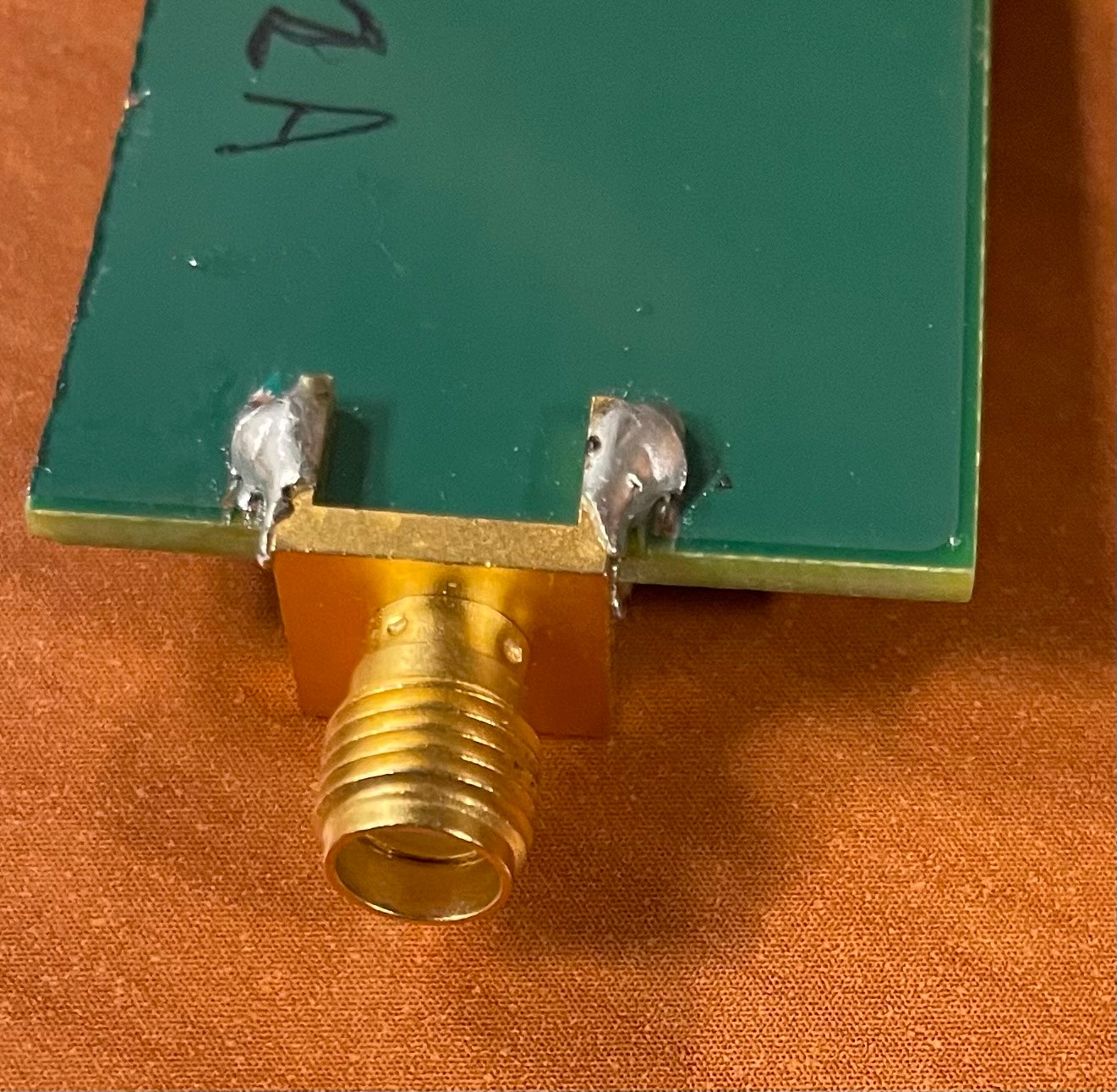
I went through the many resources available and although it helped, I still have some questions. For a microstrip, the port used is connecting the microstrip to the ground plane. However, for a loop antenna, the port connects the two open ends. I have attached a picture of the real microstrip loop antenna I am trying to simulate along with a few possible port positions. The SMA center pin connects to the excited trace and the outside pins connect to the ground on the back PCB layer. Can you tell me what port configuration makes sense?
-
August 22, 2022 at 2:55 pm
Praneeth
Ansys EmployeeHi,
Do you know for sure that experimental design has a ground trace?
If yes, then you can connect one of the arms of the loop to the ground and assign any of the port configurations.
All the very best,
Praneeth.
-
- The topic ‘How to simulate SMA connected to loop antenna on PCB board?’ is closed to new replies.


-
5059
-
1770
-
1387
-
1248
-
1021

© 2026 Copyright ANSYS, Inc. All rights reserved.


