Electronics

Electronics

Topics relate to HFSS, Maxwell, SIwave, Icepak, Electronics Enterprise and more

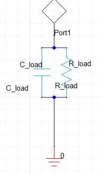
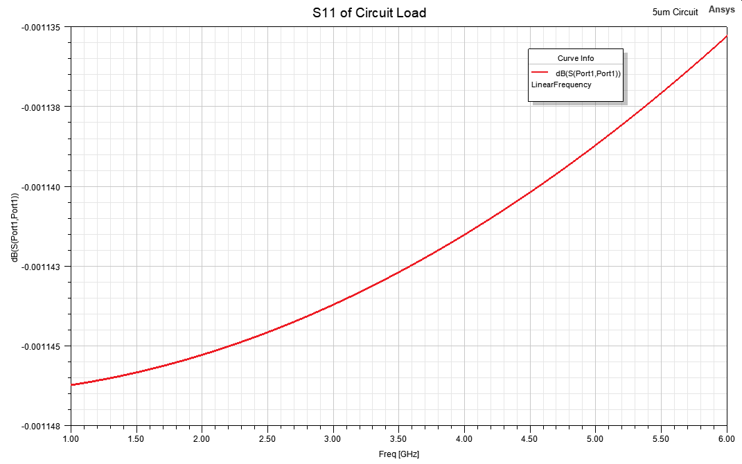
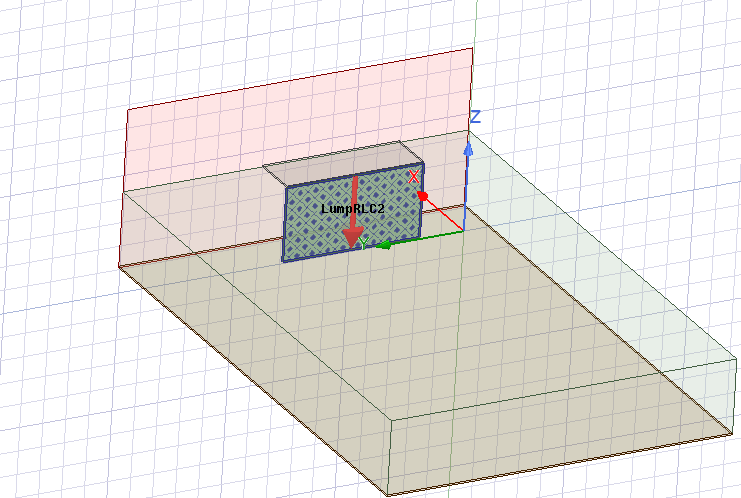
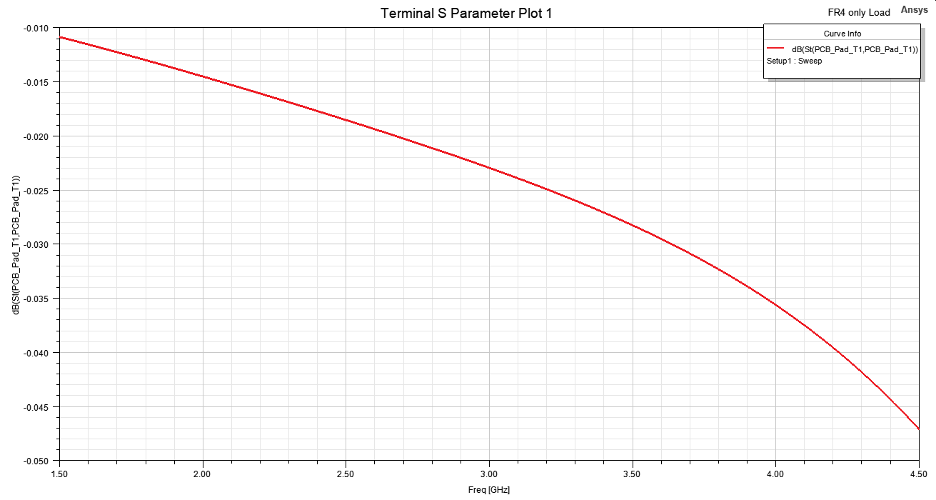
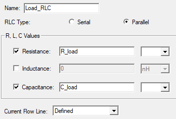
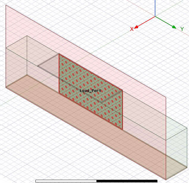
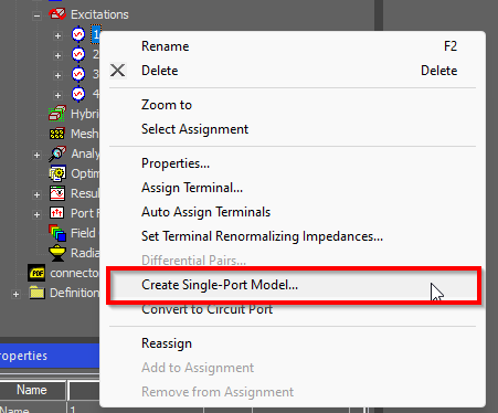
How to create Lumped RLC in HFSS to match Circuit? (Simulate load as Lumped RLC)

    • Stefano R
      Bbp_participant

      This is part of a larger project of simulating a PCB-fed resonator bonded to a lumped RLC load. I want to understand better the FEM model of the load versus the circuit representation. In the model, have a PCB microstrip wave port with Port_Z0 = 40. I want a parallel R and C (value R_load = 1MegaOhm and C_load = 40fF) shunted to the ground, as shown in the circuit diagram. Ground here is defined as the backplane of the PCB. What is the best way to connect the Lumped RLC component? These results differ from what I expected from the circuit representation.  I know the S11 values are small here, but this is just a test to see if I can model the load well.


    • Stefano R
      Bbp_participant

      I even tried replacing the lumped RLC boundary with a Lumped Port with Z = 1/(1/R + i w C) and deleting everything after the lumped port. I still am not getting good results. How would you go about simulating a lumped RLC component as shown?


    • Aymen Mzoughi
      Ansys Employee

      You can also consider creating port models for lumped ports:

Viewing 2 reply threads
  • You must be logged in to reply to this topic.