TAGGED: ansys-hfss
-
-
September 2, 2025 at 1:56 pm
-
September 11, 2025 at 10:20 am
Atsuko Kikuchi
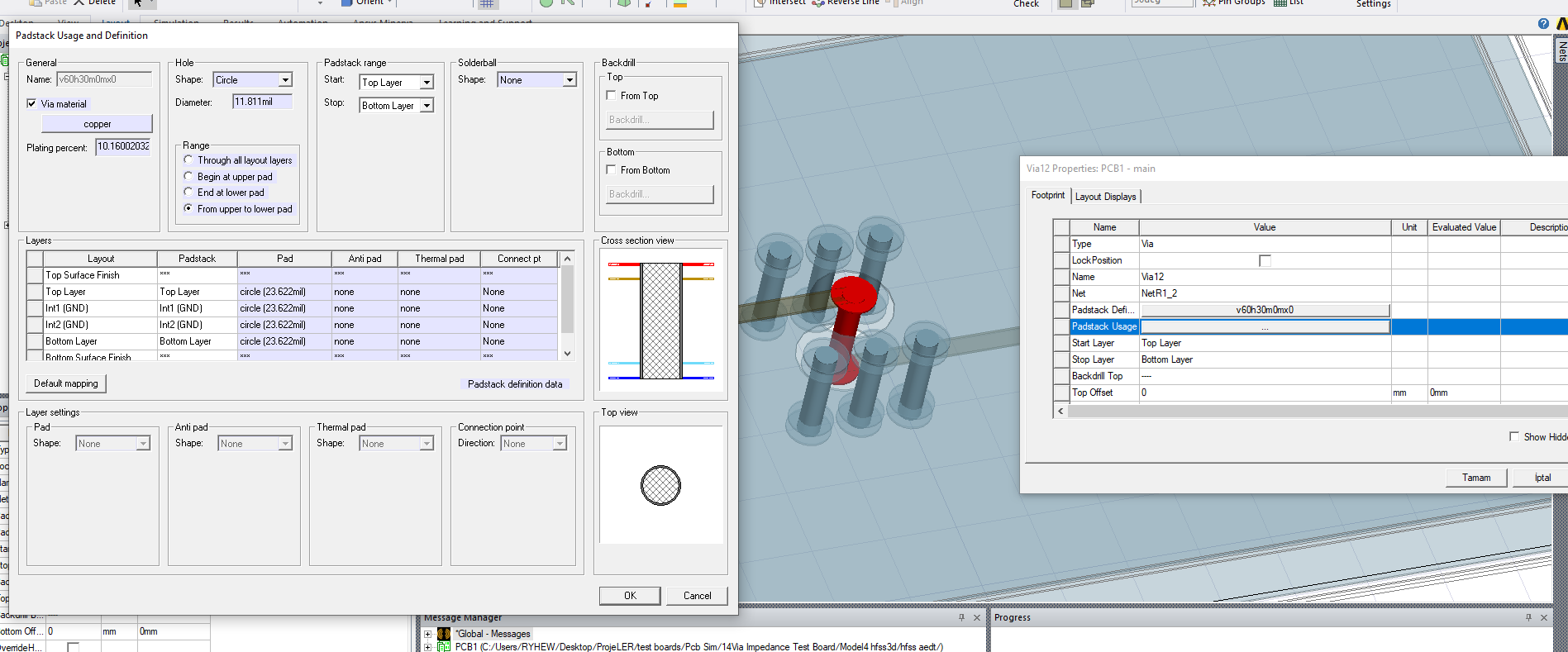
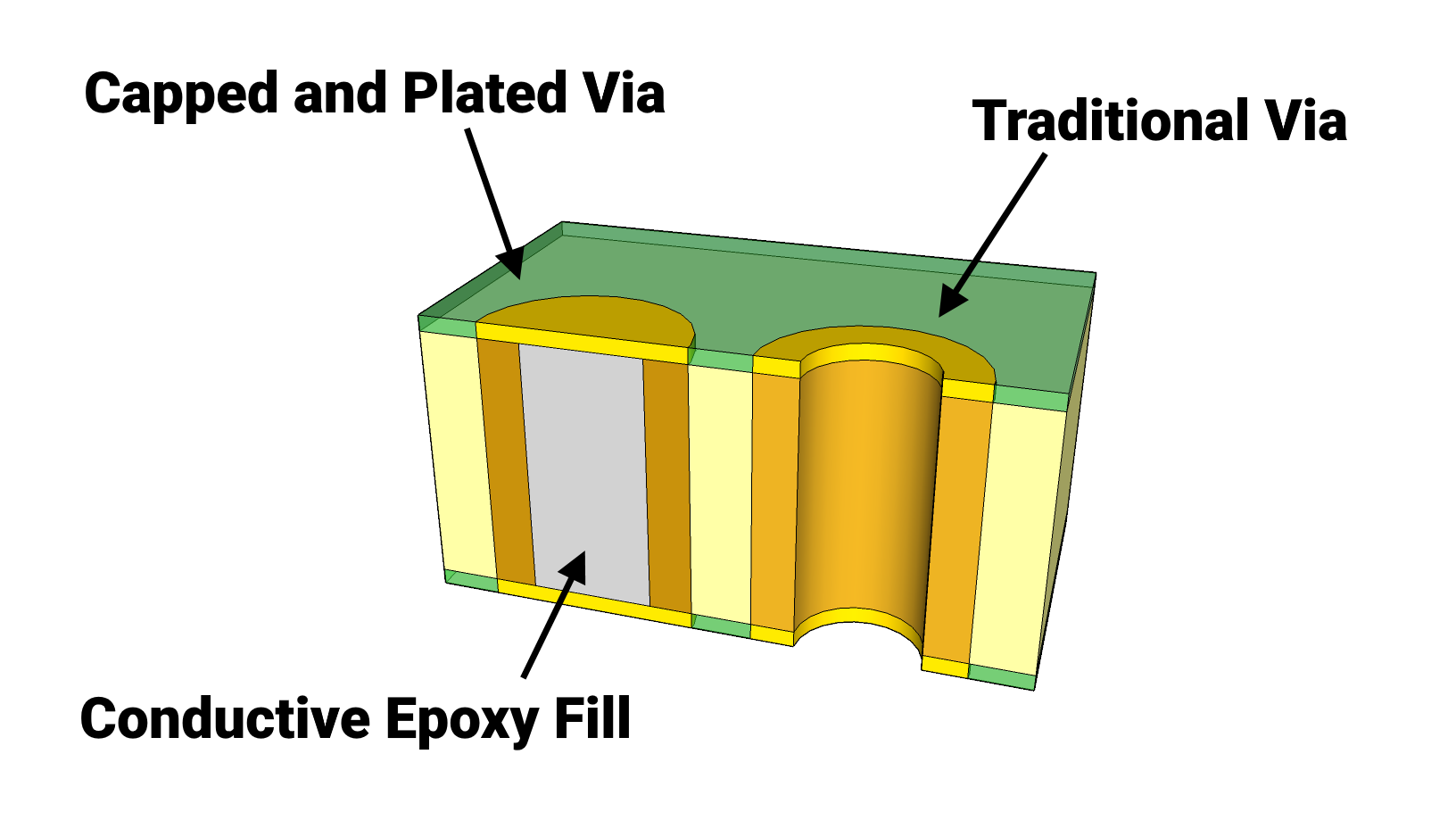
Ansys EmployeeSuch vias cannot be configured in HFSS 3D Layout. Since it is possible in HFSS, I recommend converting the design to HFSS model and simulating there.
How to export a design from HFSS 3D Layout to HFSS 3D Classic:
1. define an HFSS Solution Setup in the HFSS 3D Layout design
2. right click on the HFSS setup name in the Project Manager window and select Export -> HFSS Model...
-
Viewing 1 reply thread
- You must be logged in to reply to this topic.
Innovation Space


Trending discussions


Top Contributors


-
5274
-
1859
-
1398
-
1257
-
1021
Top Rated Tags


© 2026 Copyright ANSYS, Inc. All rights reserved.
Ansys does not support the usage of unauthorized Ansys software. Please visit www.ansys.com to obtain an official distribution.


