-
-
November 2, 2023 at 10:10 pm
Thomas Capuano
SubscriberHi,
I am trying to export my Analysis from HFSS 3D Layout to HFSS. Everything appears to transfer correctly, expect the board outline, which has a hole in it. Does anyone know how to do this operation? The help documention on board outline is sparse.
Regards,
Tom
-
November 3, 2023 at 4:52 pm
Rong Liu
Ansys EmployeeHi, Tom,
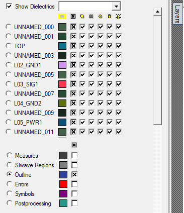
You want to have Show Dielectrics checked, then turn on only one layer one by one to find out which layer has the outline with a hole in HFSS 3D layout. The Outline layer in HFSS 3D layout won't be transferred to HFSS. What you see might be a dielectric layer.
Please feel free to open a support case. This links shows how.
/courses/index.php/courses/ansys-customer-support-space/lessons/submit-a-support-case-in-the-ansys-customer-support-space/Best regards,
Rong
-
November 3, 2023 at 4:58 pm
Thomas Capuano
SubscriberHi,
Thank you for the information.
So there is no way to export the dielectric shape to HFSS?
Tom
-
November 3, 2023 at 5:05 pm
Rong Liu
Ansys EmployeeHi, Tom,
No, the dielectric layer will be export to HFSS.
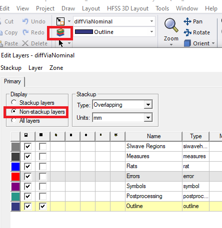
If you take a look at the Stackup setting, there are non-stackup layers, one of them is called Outline. The non-stackup layers will not be exported to HFSS. Dielectric Layers are Stacup layers, the shapes on dielectric layers will be exported to HFSS.
Best regards,
Rong
-
- The topic ‘HFSS 3D Layout Export to HFSS Board Outline’ is closed to new replies.


-
5889
-
1906
-
1420
-
1306
-
1021

© 2026 Copyright ANSYS, Inc. All rights reserved.


