-
-
October 4, 2021 at 10:09 am
areegabd
SubscriberHello everyone
I want to study the emission rate for my structure which is made of a hexagonal array of a dimer. I should place my dipole at the center of the hexagonal array. how can I have a periodic array?
best
Areej
October 5, 2021 at 1:22 amKyle
Ansys Employee
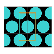
The Triangular, FCC, BCC Photonic Crystal Bandstructure example (https://support.lumerical.com/hc/en-us/articles/360041566734) demonstrates how to set up periodic boundary conditions for a triangular lattice, which I believe should be the same as your hexagonal lattice:

October 5, 2021 at 5:52 pmareegabd
SubscriberDear ,
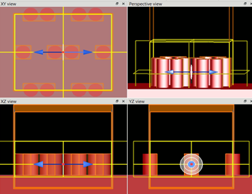
Thank you so much for your response, in fact that what I depended on when I create my array which I attached a screenshot of and I used periodic boundary along x and y. I want to make sure if it is correct or not.
Best
Areej
October 7, 2021 at 5:56 pmKyle
Ansys Employee
Ansys staff can't download attachments from the ALF, can you please copy and paste your image directly into the message, like I did in my post?
One way to tell if the image is correct is to create a geometry with multiple periods, then move the simulation region over one period in x or y. The simulation region should appear the exact same for a periodic geometry if the region is set up properly.
October 12, 2021 at 6:38 amOctober 14, 2021 at 11:17 pmKyle
Ansys Employee
Sorry, I've realized I misunderstood your original post. To study the emission from a quantum emitter like this we actually don't want to use periodic boundary conditions. When periodic boundaries are used, it is assumed that both the structure and the source are periodic, so this would model a periodic array of emitters. With periodic boundary conditions the results would include the coherent interference between the emitters in each unit cell, which would not be accurate as the emitters will be incoherent.
Instead of periodic boundary conditions, multiple unit cells should be included in the simulation region with PML boundaries. While this won't model an infinitely periodic structure, as long as enough unit cells are included the results should closely approximate a periodic structure. It looks like your non-periodic boundary simulation uses this approach, so these results would be more accurate.
I would recommend that you take a look at our OLED/LED Application Gallery examples for more details, they use a similar methodology. For example:
OLED methodology: https://support.lumerical.com/hc/en-us/articles/360042225754
OLED (2D): https://support.lumerical.com/hc/en-us/articles/360042225934
3D OLED with hexagonal lattice symmetry: https://support.lumerical.com/hc/en-us/articles/360042219294
Sorry again for the confusion. Let me know if you have any questions.
October 29, 2021 at 7:56 amareegabd
SubscriberDear Thank you so much for your Help.
Best
Areeg
Viewing 6 reply threads- The topic ‘Hexagonal periodic array’ is closed to new replies.
Innovation SpaceTrending discussionsTop Contributors-
6279
-
1906
-
1457
-
1308
-
1022
Top Rated Tags© 2026 Copyright ANSYS, Inc. All rights reserved.
Ansys does not support the usage of unauthorized Ansys software. Please visit www.ansys.com to obtain an official distribution.
-
Ansys Assistant will be unavailable on the Learning Forum starting January 30. An upgraded version is coming soon. We apologize for any inconvenience and appreciate your patience. Stay tuned for updates.


