We have an exciting announcement about badges coming in May 2025. Until then, we will temporarily stop issuing new badges for course completions and certifications. However, all completions will be recorded and fulfilled after May 2025.
Photonics

Photonics

Topics related to Lumerical and more.

Help regarding the simulation domain , monitor dimensions

    • pnair
      Subscriber

      I am working on the far field simulations of SiC thin films using dipole as the source. I have a question related to the simulation region and the height of the monitor above the simulation domain. Now, I have selected a FDTD Simulation region of 3x3x1um on my thin film which is 8x8x0.34um. Then I place a DFT monitor of 10x10x Z(um = 0.4). This means that i have placed a DFT monitor at a height of 0.4um from the surface of my simulation region. Then I preformed far field simulations for different dipole orientation. I have got farfied radiation patterns based on the above mentioned dimensions and orientations. But, when I have changed the dimensions of the FDTD simulation region (increase or decrease the dimensions of FDTD region), the far field radiation pattern also changing completely. Then, I have changed the Z-position/height of the monitor, the electric field intensity values are either increasing or decreasing. So, I would like to know how can I make sure which dimensions are correct for FDTD Simulation region, DFT monitor as the output farfield patterns is completely changing in the visualize plot. Please give suggestion to solve this problem.

    • Dimitris Polyzos
      Ansys Employee

      Hello Prabha,

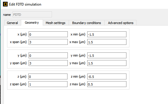
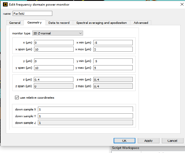
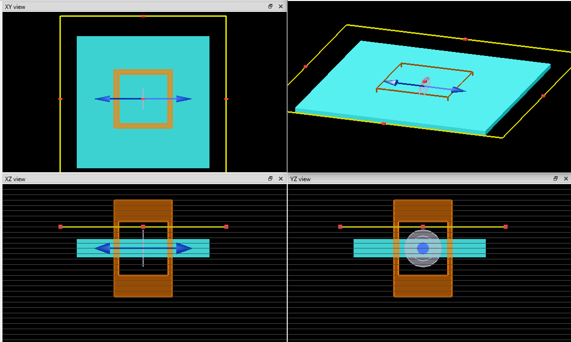
      I would be interested to see your simulation model as I am not absolutely sure if you have set correctly the FDTD span and the monitors. However, I believe that the transmitted fields correspond to scattered fields, then I reckon that you should place the monitor close to the source. From size perspective, monitors should be large enough in order not to "cut " the transmitted fields. If that is not applied, then the transmission will not be correct. For the same reason you should position the monitor fairly close to the structure. Actually, the further away the monitor is, the wider it should be to encompass the diffracted fields without truncating them. I would set the monitor to be as large as the FDTD region.
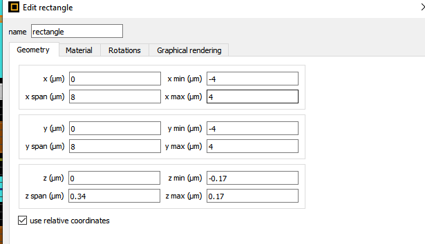
      For the source, I don't think it really matters, as long as it is big enough to includes the full aperture. So the following things should be considered regarding the accuracy of the far field projections:

      • the accuracy of the FDTD calculation itself (mesh)
      • the field truncation at the edge of the monitor/simulation region

      Lastly, make sure the FDTD region is big enough: if the PMLs are too close to the aperture, they may affect the evanescent fields. Half of the larger wavelength of interest is usually a good starting point, but you may want to validate this by varying the size of the FDTD region and see how it affects the results. Please refer to the following articles:

       Integrating power in far field projections

      farfieldfilter - Script command

       Using spatial filtering to avoid truncating fields in far field projections

      I hope I helped.

      Kind regards

      Dimitris

    • pnair
      Subscriber

      Hello,

      Thank you for the reply.But, I am not clear about the FDTD simulation span and why the output results are varying for different simulation volume. I have SIC thin film of thickness 340nm. So, I have assumed it is infinitely long in x&y directions. Then I have selected a FDTD Simulation region of 3x3x1um on my thin film which is 8x8x0.34um. Then I place a DFT monitor of 10x10x 0.4 This means that i have placed a DFT monitor at a height of 0.4um from the surface of my simulation region..please see the attached screen shots of the geometry of the structure.


      This is how I have set up the simulation window and monitors. But, the issue is that If I am changing the simulation volume, the the farfield emission pattern is also changing. Please suggest if there is any way to solve this problem.

    • Dimitris Polyzos
      Ansys Employee

      Hello Prabha, 

      Thanks for your reply and sharing these screenshots. 

      I reckon that you should decrease the z span of the simulation region similar to this article: Always-extend-structures-through-PML-boundary-conditions.  I assume that reflection froom the bottom part of your structure might affect the E field. Also, is there a particular reason of using diple source? I assume that with a plane source (extended out of FDTD BCs) would provide a good starting point to check if there is a  variation in far field results when you change the FDTD spa.

      Also, all BCs could be set to PMLs as there is no periodic structure on the SiC film. Thus, you can simulate the structure considered to be infinite in x,y direction. Another comments is that ideally for dipole source you should use Dipole-source-Simulation-object a box monitor. You could try these steps to measure the field:

      • Run the simulation using just a dipole alone, and then record the field by using a box monitor. 
        Far field projections from a box of monitors
      • Do farfield projection from the box monitor to a plane in front of the structure and save the  projected farfield into a dataset.
      • Run another simulation by using the field from previous step as an import source, and measure the field around the structure Import source - Simulation object

      An alternative would be to use STACK solver, as I can see that your simulation model is a thin film without patterned structure. Please refer to these articles to check how you can exploit them and run your simulation:

      Reflection-calculation-using-a-dipole-source

      Simple-far-field-projection-example

      Reflection-calculation-using-a-dipole-source

      I hope I helped. PLease let me know if something of the above is not clear and if I can furhter help you.

      kind regards

      Dimitris

    • pnair
      Subscriber

      Thank you for the reply. I have gone through the above mentioned suggestions. But, I am still cofused with the above-mentioned problem. I need to use a dipole source with three different orientations to calculate the total electric field by finding the average. I know that dipole radiate power in all directions. I am using PML boundary conditions in X,Y & Z directions.I am using a Z-normal monitor to record my field and placed within the boundary conditions just above the source as shown in the above picture.I don't know is it OK to use Z-normal monitor to record the dipole power but i am assuming  it is large enough to record all the field data. I have already mentioned the dimensions of FDTD region-monitor-thinfilm that i have used to generate this farfield pattern .  So, I need to study the far field data using the dipole source. And, I got a farfied emission result as shown below

      But, if i change the dimensions of the FDTD region/simulation region. Then my far field data and emission pattern also changes.


      This is how i have changed the FDTD/simulation volume and also I placed the monitor a little bit higher than the previous one. Then my farfield emission pattern also changes. So, now i am confused how can i decide the simulation/fdtd region. Is there any specific script about how to select a FDTD region and where to place the monitor which i can study as a reference to place a dipole source on a thin film and to study farfield data. I have followed all the videos and manual for this. But, it didnt help me that much to solve this issue. 

    • Dimitris Polyzos
      Ansys Employee

      Hello Prabha, 

      Sorry for the late reply. 

      It seems that the intensity of the farfield pattern is at the scale of 1e-14 upt to 1e-27. My comment here is that these values are negligible and can be considered noise. Please try to increase the intensity of the dipole source or add various diploe sources in the simulation region and conduct a convergence testby increasing the intenisty of the source nad checking the point where the emission pattern doesn't change.

      I hope I helped.

      Kind regards

      Dimitris

Viewing 5 reply threads
  • The topic ‘Help regarding the simulation domain , monitor dimensions’ is closed to new replies.