-
-
March 1, 2024 at 4:15 pm
pnair
SubscriberHello,
I am working on the farfield simulations of SiC thin film using dipole source. I have attached a screen shot of my device structure here. My issues are with the orientation of the dipole source and far field emission patterns. So, I am getting same farfield emission pattern for x-dipole orientation and y-dipole orientation. But, in theory of the dipole source, the farfield emission pattern should be different for x& y dipole orientation. Could you please help me regarding this?
This is the thinfilm structure used for the simulation,
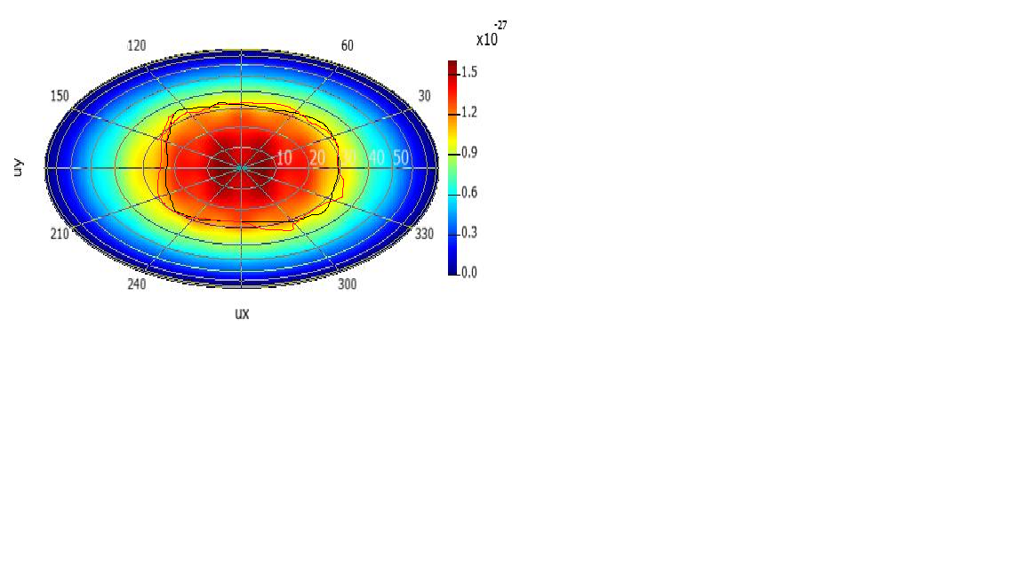
This is farfield plot for y-rientation of the dipole.
This is the farfield emission pattern for x-orientation of the dipole
How is it possible to get the same farfield emission patterns for x & y-dipole orientation?
Thank you.
-
March 5, 2024 at 5:37 pm
Guilin Sun
Ansys EmployeeIs the thin film in xy plane? if so, x/y polarization will have the same radiation since it is rotationary symmetry.
-
March 20, 2024 at 6:45 pm
pnair
SubscriberThank you for the reply. Could you please elaborate a little bit about the rotationary symmetry? Is it related to the polar-azimuthal angle in the farf field emission plots?
-
March 20, 2024 at 8:00 pm
Guilin Sun
Ansys EmployeeFor planar structure like thin film, it is unifrom in a plane, for example in xy pane. In such case, a dipole polarized along x and y will have the same radiation, since they "see" the structure the same. That said, for 90 deg rotation symmetry of the structure, the dipoles will behave the same. I hope this helps.
-
March 21, 2024 at 9:20 pm
pnair
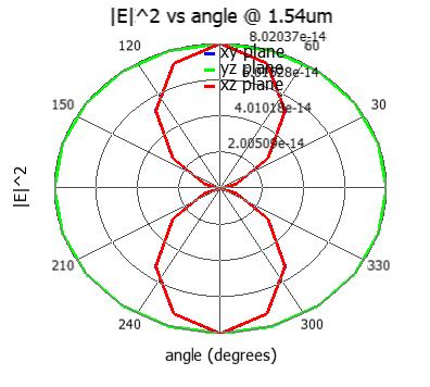
SubscriberI would like to clarify further about this. For example I have done the dipole simulations using box of monitors for a) dipole along X-direction by giving phi=0 and theta = 90 b) dipole along y-direction by giving phi=90 and theta =90. Then i get the following 2D plots.
1) For x-dipole orientations
2) For Y-dipole orientations
If i take the X-Y plane in both the cases, then both the emission patterns are different. There is 90-degree shift in the pattern. Why this is not the case with the dipole simulations on a SiC thin film and both the X&Y-dipole orientation plots seems to be the same?
This is farfield plot for y-rientation of the dipole.
This is the farfield emission pattern for x-orientation of the dipole
Am I intrepretting the farfield plots wrong for x&y dipole orientation? Is it possible to seperate x-y , y-z & X-Z planes from these spherical polar plots to see how the pattern looks or is similar to the box of monitors plots?
-
March 22, 2024 at 3:30 pm
Guilin Sun
Ansys Employee" There is 90-degree shift in the pattern." this is reasonable, as the two planes does not have a common reference angle. from the 3D farfield projections it is clear that the radiation rotated 90 deg (due to meshing). otherwise they are the same. I would like to suggest to check the 3D donut-shape radiation pattern from theory.
-
March 22, 2024 at 3:59 pm
Guilin Sun
Ansys Employee3D projection and e x-y , y-z & X-Z projection are different. You can get a cut form 3D radiation pattern: Creating line plots of far field projections
-
March 25, 2024 at 9:34 pm
pnair
SubscriberHello, I have made a cut to create a line plot from 3D radiation pattern as suggested here for theta=0 & phi=0 to 360. As based on dipole radiation pattern theory for x & y-dipole orientations, there shouldn't be any value for phi=90 and phi=270. but i am having same value(5.6e-14) for all angles of phi. I have used the above-mentioned 3D poalr plot to create line plots. Is it due to the meshing i have used for the simulations?
-
March 25, 2024 at 9:51 pm
pnair
SubscriberI mean based on the dipole radiation theory, for x-dipole orientation, I shouldn't get any field values for phi=90 and phi = 270. But, i am getting same values for phi=0 to phi=360 for theta=0. It seems like a circle in the 3D radiation plot for x-dipole orientation.
I have marked the region for the above question in 3D plot. Am i interpreting this 3D plot wrong? For me, there is same value for phi=0 to phi=360 at theta = 0.
-
March 26, 2024 at 12:03 am
Guilin Sun
Ansys EmployeeThe monitors should be carefully aligned to capture all the radiation.
The PML should be far away from dipole source and PML should be thick enough. The scattering polar plots show the result is correct, except the rotation.
It seems your question is different from your original post.
-
- The topic ‘Help regarding dipole simulations’ is closed to new replies.


-
5704
-
1896
-
1419
-
1305
-
1021

© 2026 Copyright ANSYS, Inc. All rights reserved.


