Ansys Assistant will be unavailable on the Learning Forum starting January 30. An upgraded version is coming soon. We apologize for any inconvenience and appreciate your patience. Stay tuned for updates.
Electronics

Electronics

Topics related to HFSS, Maxwell, SIwave, Icepak, Electronics Enterprise and more.

Evaluating loss using Eigenmode and Modal Network

    • gobbo.marco98
      Subscriber

      Hello everyone,

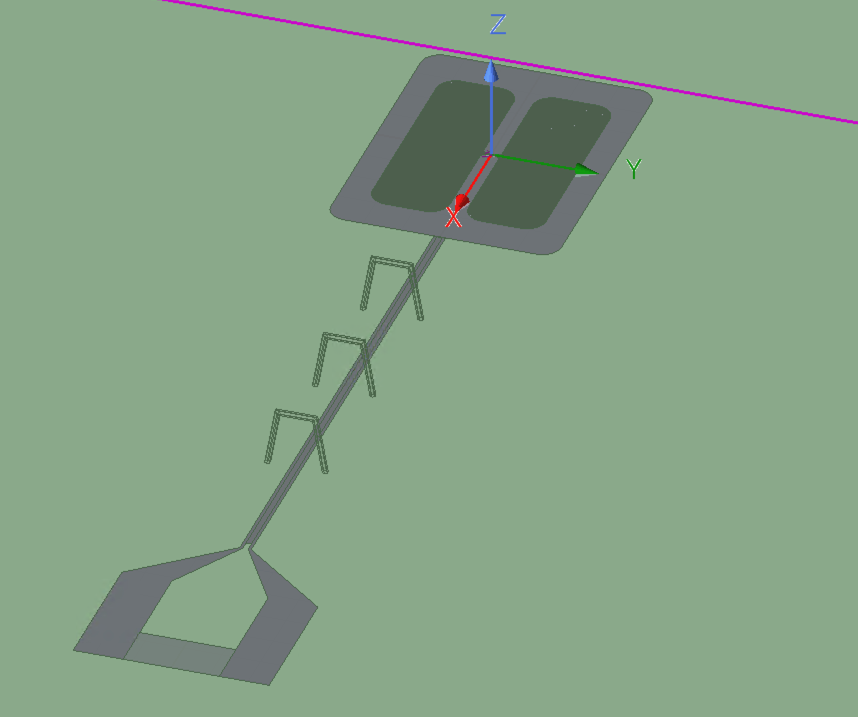
      I am trying to compare the loss of a lumped LC resonator coupled to a shortened CPW line placed in different positions relative to the resonator.

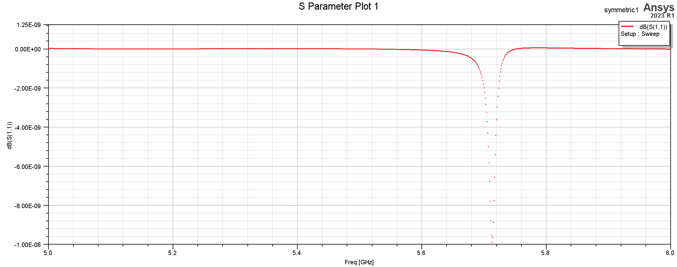
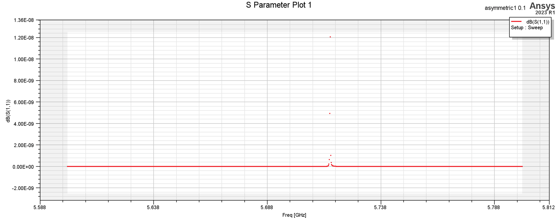
      First, I performed an Eigenmode simulation where I modeled the external loading by assigning a lumped RLC boundary of 50 Ω at the launcher of the CPW line. With this setup, I obtain a mode at approximately 5.717 GHz with a Q of about 5.47e5.

      Then, I ran a Driven Modal (Modal Network) simulation by assigning a lumped port (50 Ω) for the Excitations at the same launcher and sweeping from 5 to 6 GHz. In this case, I observe a feature close to the expected frequency (~5.7 GHz), but the dip in S11 is extremely shallow (on the order of 1e-8). The result is also not very stable: depending on the parameter sweep, sometimes I see a dip, and sometimes even a peak instead.

      I expected that by fitting the S11 feature I could extract a linewidth consistent with the Q obtained from the Eigenmode simulation, but this does not seem to be the case.

      My questions are:

      • Are Eigenmode and Driven Modal simulations directly comparable in this context?
      • Should I expect to extract the same linewidth from S11?
      • Or am I missing something in the Driven Modal setup or in how I am interpreting the results?

        I attach here the design and two S11 profiles, as you can see, the structure is relatively simple: a resonator coupled to a shortened CPW line, with the launcher used as the boundary/excitation port.

        Thanks in advance for any help or suggestions!

    • Takeshi Itadani
      Ansys Employee
      The second dB(S(1,1)) graph shows that the S-parameter exceeds 0dB. Since it appears that no active elements are implemented, this analysis result is abnormal.
       
      It is possible that the analysis accuracy itself is insufficient. Try reducing the Maximum Delta S, increasing the Maximum Number of Passes, Minimum Number of Passes, and Minimum Converged Passes, and increasing the number of Adaptive analyses.
       
      Also, are you using materials with defined tanδ, or are you setting the load impedance as a complex number? If so, please check by defining the S-parameter as power. Select HFSS > Design Settings... and then select Power in the S Parameters tab.
    • gobbo.marco98
      Subscriber

      Thanks for your reply.

      For the solids, I'm using a PEC for wirebonds, silicon for the substrate, and vacuum for the volume in which to evaluate the simulations.

      For sheets, I have a PEC for the metal, an RLC Boundary for the inductor between the two islands, and a Lumped Port with 50 Ohms of impedance. In the Lumped Port window, I also do a Port Renormalization with a Full Port Impedance of 50 Ohms.

Viewing 2 reply threads
  • You must be logged in to reply to this topic.
[bingo_chatbox]