TAGGED: convergence, Lumerical-CHARGE, semiconductor
-
-
March 12, 2024 at 2:38 pm
sicli21
SubscriberHi,
I want to simulate E field in the geometry attached. Greens are metal layers where I define my BCs, purple is waveguide, and blue is SiO2 semiconductor material.
With current material properties, simulation gives an error message
The error code is 9010, the process number is 0
Recombination and KdotP are disabled. I tried to change Ec Valley to X or L. When I close material window and open it back I see Ec valley unchanged. I increased global iteration limit and changed solver type, non worked.
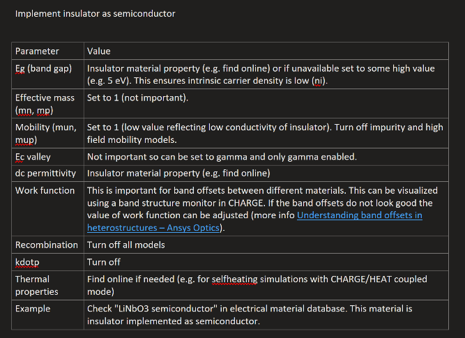
How can I configure non-semiconductor materials to semiconductors ? My designs have insulator cladding and my waveguide is also another semiconductor material that I disabled all recombinations to make it work. I am only interested in Electric field distribution
-
March 12, 2024 at 4:24 pm
Amrita Pati
Ansys Employee-
March 12, 2024 at 4:32 pm
sicli21
SubscriberHi Amrita, I am already doing that for my waveguide. But my waveguide and metal contacts seperated by a cladding insulator material SiO2 50umx10um. So, I also modify cladding as semiconductor but get an error of
The error code is 9010, the process number is 0
-
-
March 12, 2024 at 4:34 pm
Amrita Pati
Ansys EmployeeDo you require the field distribution only in the waveguide or in the cladding as well? Can you check the log file (saved in the same directory, has the name filename_p0.log) to provide more details of the error?
Regards,
Amrita-
March 13, 2024 at 11:24 am
sicli21
SubscriberI need field everywhere. Log file
Remote execution (remote argument) set to true.
Generating mesh.
Mesh generation complete (1s)
+ vertices: 6696
+ elements: 13299
All processes are communicating and ready to proceed to simulation…
Starting solver.
The program terminated due to an error: Initialization failed to converge charge update due to numerical failure. For instructions on how to troubleshoot this issue, please refer to this: online reference
Error: there was an unknown parallel error. The error code is 9010, the process number is 0My waveguide and cladding are semiconductor. I realized that if I make them same material I don’t get any errors. So, configuration of the materials as semiconductor must be correct. Increasing iteration limit, changing solver type, enabling backtracking, and other methods mentioned in the convergence errors article don't help
-
-
March 13, 2024 at 6:02 pm
Amrita Pati
Ansys EmployeeHi,
I will look into it and get back to you.
Regards,
Amrita -
March 14, 2024 at 4:52 pm
Amrita Pati
Ansys EmployeeHi,
I briefly discussed this with my colleague. Since CHARGE was designed to solve Possion and Drift-Diffusion equation in semiconductors, it can be more challenging to solve them in insulators (although as semiconductors). The electric fields will be returned everywhere in the material, but CHARGE needs at least one active semiconductor region to be able to work. So, I will recommend you to keep the SiO2 cladding as an insulator and just make the waveguide a semiconductor. Let me know if that helps.
The error message is also generic, so it can be due to several reasons. But let's try the first step and see if there is any improvement.
Regards,
Amrita-
March 15, 2024 at 10:42 am
sicli21
SubscriberThank you for your response. In https://optics.ansys.com/hc/en-us/articles/360042326694-Ferroelectric-modulator , it says
"""
Due to the same reason as the one mentioned above, the Si layer in the waveguide also requires a voltage boundary condition. Instead of providing the boundary condition directly from a contact (gnd) we provided the boundary condition through another semiconductor region
"""
If I make my SiO2 insulator, my semiconductor waveguide won't have any BC and according to the example that may cause inaccurate results.
-
-
- The topic ‘CHARGE – Creating SiO2 Semiconductor’ is closed to new replies.


-
6104
-
1906
-
1436
-
1308
-
1021

© 2026 Copyright ANSYS, Inc. All rights reserved.


