-
-
August 12, 2021 at 7:43 am
anshuman.kumar
SubscriberHi,
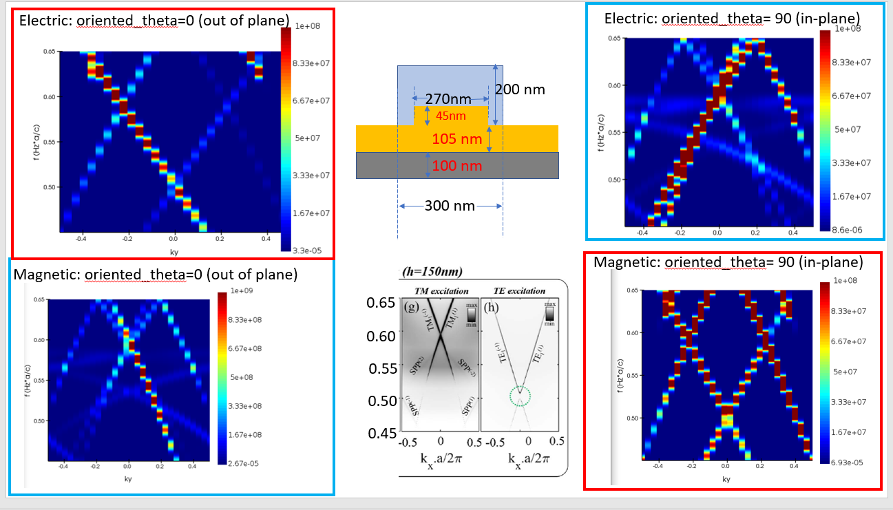
I want to plot bandstructure for a dielectric grating structure as shown in the screenshot. I was having trouble with separating TM and TE modes while using the standard dipole cloud with random orientation. However, the discussion: /forum/discussion/comment/116911#Comment_116911, it says that for bandstructure, the dipole cloud has to be oriented out of plane (theta=0) and then by toggling between Magnetic and electric dipole, we can get TE and TM modes, respectively.
However, in my case orienting the dipoles (by fixing theta) is indeed helping in preventing the mixing of TE and TM modes but if you see the screenshot attached, Magnetic dipole_cloud oriented out of plane (i.e. theta = 0) is giving bandstruture similar to TM mode while Magnetic dipole_cloud oriented in-plane (theta = 90) is giving results similar to TE mode.
Similar case is being observed for electric dipoles.
August 12, 2021 at 8:35 pmGuilin Sun
Ansys EmployeeBoth electric and magnetic dipoles may excite modes of different polarization, but one may be more efficient than the other. In order to separate the TE and TM modes, you may try to use different symmetry BC, which will definitely get ride of the other polarization, provided that the geometry has symmetry, and in your case, I think it has. please try and let me know if it works.
August 18, 2021 at 8:07 amSubscriberHi,
Thanks for your response. Just to recall...
I am working on a 2D simulation, where I have a dielectric grating over a metal layerand I am looking for bandstructure with TE mode only.I have oriented dipoles out of plane for TE mode calculation but stillgetting some extra modes, for which you suggested touse symmetry in your last comment.Could you please help me in setting symmetry boundary conditions in my simulation.
 I have used Bloch boundary conditions in y-direction and PML in x-direction.
Could you please suggest how to use symmetry to separate TE modes from others.
August 18, 2021 at 6:26 pmAnsys EmployeeFrom your previous post, I guess it was 3D, so to suggest the symmetry BCs.
In 2D case, TE and TM are well defined so you can choose proper type of dipoles and polarization to get the bandstructure. However from the screenshots, it seems the waveguide cladding and substrate have limited size? which periodicity you are expecting? the period should be along the length of the waveguide, whereas the gladding and substrate should be large enough to be truncated by PML, instead of having air. I guess it is because of this . Please try to modify.
This cross section:

has mode confinement in 2 directions, so the periodicity should be along the 3rd dimension, the length of the waveguide.
Please make sure you are simulating correct physical device.
Viewing 3 reply threads- The topic ‘Bandstructure calculation for TM and TE mode’ is closed to new replies.
Innovation Space Trending discussions
 Top Contributors
-
peteroznewman
 5194
5194 -
scabo
 1859
1859 -
Dennis Chen
 1387
1387 -
javat33489
 1250
1250 -
Shyam Prasad V Atri
1021
Top Rated Tags
© 2026 Copyright ANSYS, Inc. All rights reserved.
Ansys does not support the usage of unauthorized Ansys software. Please visit www.ansys.com to obtain an official distribution.
-
Ansys Assistant will be unavailable on the Learning Forum starting January 30. An upgraded version is coming soon. We apologize for any inconvenience and appreciate your patience. Stay tuned for updates.