Electronics

Electronics

Topics related to HFSS, Maxwell, SIwave, Icepak, Electronics Enterprise and more.

Appropriate way to assign excitation to a Log-Periodic-Dipole (Wire)-antenna.

    • sahas
      Subscriber

      Hello peers, I have been trying to simulate and observe "directivity" of a LPDA antenna as portrayed in the attached image on the left corner. This is comprised of wire dipoles. 

      There are two things I have been extremely concerned of,

      (1) How to assign excitation appropriately to the LPDA ? Shall it be "lumped port" at the top via "rectangular sheet" with defined line ? or shall I make these wires hollow and then apply "wave port" ??  So, essentially, how to assign excitation to my LPDA structure ?

      (2) Often I have observed a stud at the bottom connecting the booms. So, do I have to connect the bottom of the boom with some wire or pec material ? 

      Kindly, please have your valuable extertise. Thanks. 

    • AncS
      Ansys Employee

      Hello Sahas,

      You can assign lumped port excitation for your LPDA. To learn more about the excitation types, you may go through the AIC course -  'Ansys HFSS Port Types - ANSYS Innovation Courses '

      You can try simulating 'Log Periodic Dipole Array (LPDA)' from the Antenna Toolkit ACT extension which is easier to use, for your reference.

      Hope this may help.

      Anchal

      Ansys

      • sahas
        Subscriber


        Dear Ma’am,

        Thanking you for your kind response. 

        I completely understand that lumped port has to be attached but the concern is how may I put it on the structure. Unlike CST, which I have been long using, Lumped port is also messing up S-parameters, I have checked that in case of a “Fat” Pipe dipole and compared with CST. 

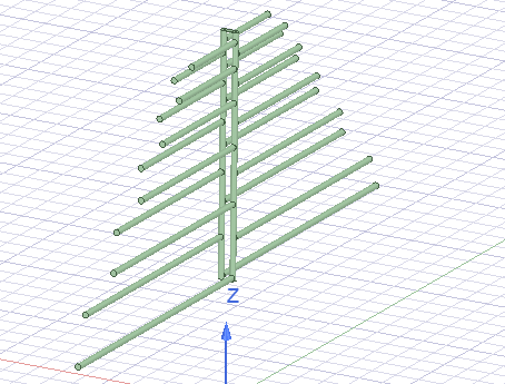
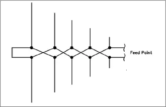
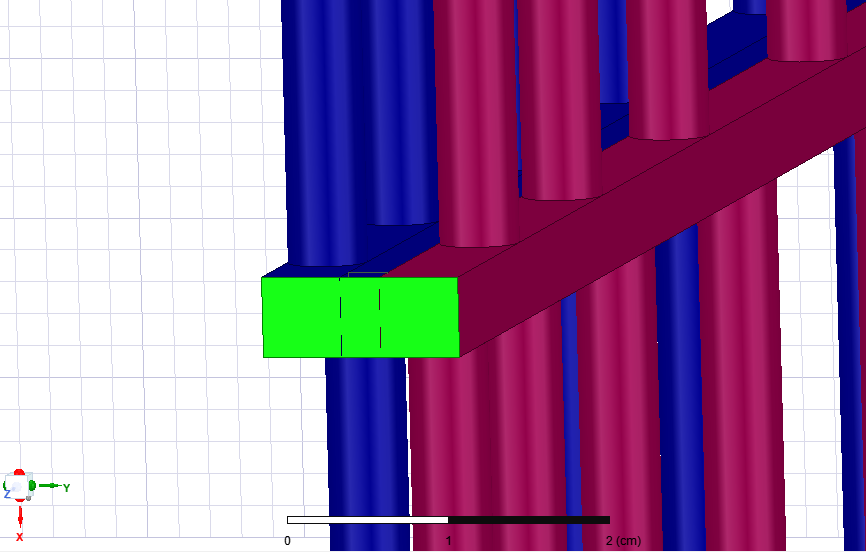
        The signal is to be fed from the top of the structure of each boom. So do I need to assign 2 lumped ports over the top faces of 2 booms with 180-deg phase shifted (like in the figure 1), here two greenish squares are representing two different lumped ports. The integration lin is upward in first port and downward in second port.

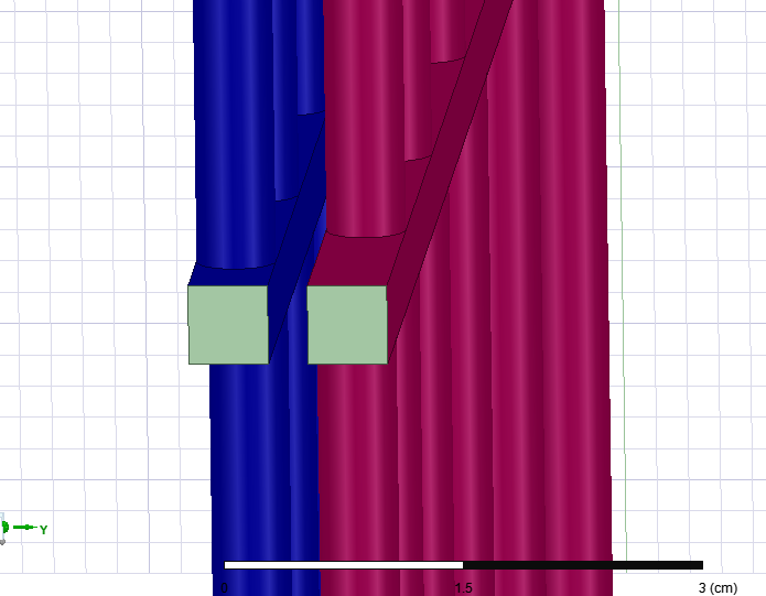
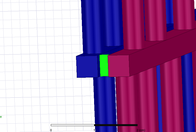
        Or shall I connect a single “Lumped port” covering the faces of both the square booms and the integration line to be difined from the center of face of boom 1 to center of face of boom2, as shown in the 2 figures below.


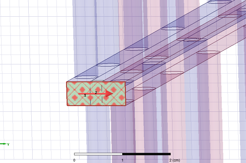
        Or, Do I have to connect the lumped port in such a way so that it connects both the booms by-side as show in the figure below.

        Although, I have tried all these ways to assign the excitation but didn’t find expected results. So, I presume that I might be missing something here. Kindly, let me know about it.

        Also, simple “stub” drawing essentially works in CST but here it is not working and therefore I have attached a Lumped-“series”-RLC element (R=300 ohms, L=C=0) at the bottom of the booms as last figure (but at the bottom), so that the rectangle touches sides of the two booms, Integration line has been drawn from the surface of first boom to second boom. Is it the correct way to assign the lumped-load ?

        Kindly let me know where am I possibly comitting mistake and how to fix that.

        Thanking you a lot.

        Warm Regards.

        Subhadip.


    • AncS
      Ansys Employee

      Hello Sahas,

      Can you please check if an open boundary condition or any equivalent boundary to absorb the fields radiated from the antenna is defined in your model?

      You can try simulating 'Log Periodic Dipole Array (LPDA)' from the Antenna Toolkit ACT extension which is easier to use, for your reference.

      Hope this may help.

      Regards

      Anchal

Viewing 2 reply threads
  • The topic ‘Appropriate way to assign excitation to a Log-Periodic-Dipole (Wire)-antenna.’ is closed to new replies.