-
-
September 27, 2023 at 4:10 pm
Yoon Jung
SubscriberWhen designing a thin conductor with a very large width compared to its thickness, is it possible to do it in 2D? I've heard that the result is not much different than in 3D, but it is faster.
If I want to layer two different types of conductors, how do I set the thickness while drawing in 2D? If I set the material in the same place and in finite Conductivity, I get an error that the boundaries overlap.
-
September 28, 2023 at 6:51 pm
HDLI
Ansys EmployeeHello Yoon,
2023R1 Maxwell 3D DC conduction solver would support thin layer boundary with thickness and conductivity. Please check it. Thanks.
HDLI
-
September 28, 2023 at 8:19 pm
Yoon Jung
SubscriberThanks for the answer. But I have to simulate with hfss.
I think it's finite conductivity or layered impedance, is that right? When I simulate thin conductors in 3D, the results are completely different. I don't know why.
-
-
September 29, 2023 at 7:39 pm
Faezeh Ladani
Ansys EmployeeHi Yoon,
If you have structure where these thin layers are very close, making narrow gaps, then using 2D sheets would understimate the capacitance of such gap. There might be other scenarios which 2D approximation can have some impact on the results. At the same time, it can speed up the simulation significantly. There are also other factors, like how thing the metal layer is compared to sking depth, or are we assigning it two-sided or one-sided boundary... Feel free to search these topics on HFSS online help to learn more about. To provide more specific discussion, we need to learn more about the project you are doing and possibly investigating the model, which leads to submiting your case for technical support.
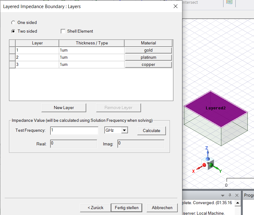
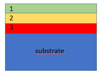
In general, when you have more than one layer (one material), you need to assign Layered impedance boundary. There you should be able to assign thickness and material properties to each layer.
-
September 30, 2023 at 12:29 pm
Yoon Jung
Subscriberhi. Thanks for the answer. I’m working on it now with layered impedance. I was wondering what is the order of the layers?
When I layer on top of the substrate like this,
In this picture I drew, is number 1(color green) gold or copper?
For me, this order is important. If I change the order, the result is different.
-
-
October 3, 2023 at 7:17 pm
Faezeh Ladani
Ansys EmployeeHi Yoon,
Layer 1 is on the top, based on the normal vector of that face. The direction of the Normal may depend on how the object is created. To make sure which direction is the top, you can move the face along Normal (Select the Face, from menu: Modeler>Surface>Move Faces>Along Normal...
-
- The topic ‘2D with thickness’ is closed to new replies.
- Ansys Maxwell 3D – eddy current
- Maxwell circuit – PWM
- Plotting Ex, Ey and Ez in vector forms individually
- Simplorer+Maxwell Cosimulation results and Maxwell results mismatch
- Compute near field simulation with current
- Ansys-MATLAB Co-Simulation
- Y wiring method and the start and end points of winding.
- Ansys Resonance simulatioin error
- Calculating E-field tangential to a 2D resonant structure on a sapphire chip
- How does Ansys Twin Builder implement different simulation steps for subcircuits
-
2262
-
925
-
599
-
591
-
497
© 2025 Copyright ANSYS, Inc. All rights reserved.