Ansys Learning Forum › Forums › Discuss Simulation › Photonics › Query related to Rough waveguide 3D FDTD, Simulation time, Negative Transmission › Reply To: Query related to Rough waveguide 3D FDTD, Simulation time, Negative Transmission
Hi,
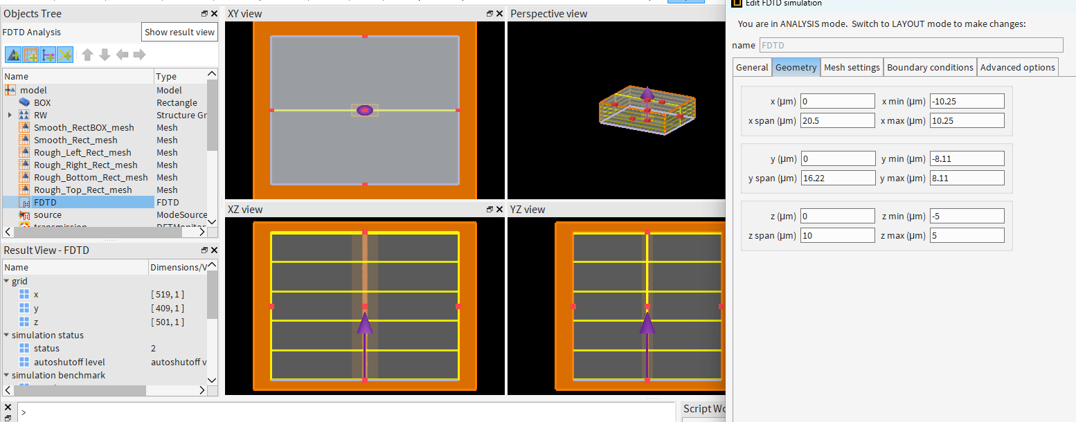
The simulation geometry is quite big. X=20.5ym, Y=16.22um and Z=10um as shown in the figure. I will try to use cluster to run the simulations.
I have a few questions, as I am using PML boundaries and it can be seen that PML boundaries are very close to the DFT monitor at the input and Mode expansion monitor at the output. Does changing the number of PML boundaries also changes the results? Is it still possible to have reflection, if I am considering 48 PML boundaries?
Shall I move away the simulation region (PML Boundaries) from the input and output location as well, i.e, in the propogation direction? What may be the ideal distance between the monitor and PML boundaries to keep the reflection min (atleast 4-5 order less)?
When I consider the ports, does it provide the results in Fundamental model or in total power/transmission?
It is possible to accurately capture the scattered power/transmission from the surface roughness perpendicular (X-Y plane) to the propogation direction (Z axis)? How?
Can I also simulate the surface roughness in VarFDTD?


