Ansys Learning Forum › Forums › Discuss Simulation › Photonics › Simulation of pulsed light input germanium silicon detector › Reply To: Simulation of pulsed light input germanium silicon detector
Hi Amrita,
First of all, thank you for your attention and answers to my questions.
I will answer your questions one by one.
1.The plused light source setting in the FDTD
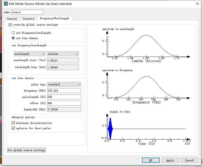
I set the light source to a pulsed light by set the source from "set frequency/wavelength" to "set time domain" in the settings of the mode source, and then set the parameters like the picture below.(It warned me that the image is failed to upload cause a XHR Transport error, but it seems ok on my page, so I'll state the parameters just to be on the safe side.)
pulse type:standrad
frequency:193.414
pulse length:200
pulse offset:400
2. The absorbed power calculated by FDTD
During this period of time, I have read the code of the analysis group for calculating the absorbed power and calculating the photogenerative carrier generation rate. My current understanding is that the photogenerative carrier generation rate obtained from the FDTD result analysis is a linear result for the power of the light source, that is, if the other parameters of the light source are unchanged and only the amplitude is adjusted, The photogenerative carrier generation rate and the optical power absorption rate are always the same because they are both normalized to the input amplitude.
3. The space charge shielding effect in the charge simulation
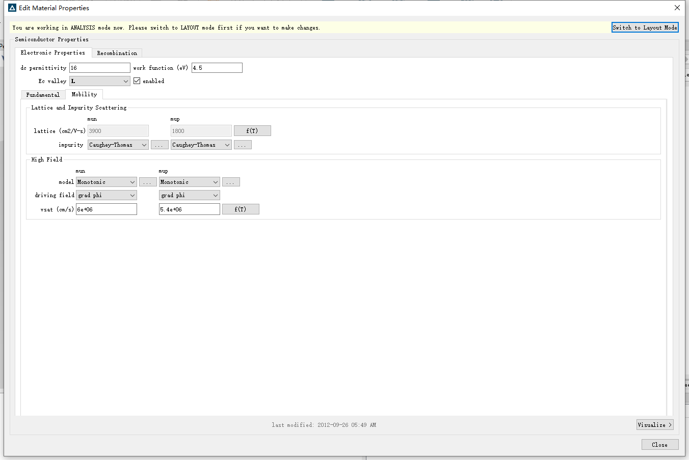
I mentioned before that I did not see the calculation formula of mobility in Charge solver. Later, I looked it up on the official website and found the description of the calculation process of Material mobility parameter from the introduction of Semiconductor Material Model Properties. Through reading this part, My understanding is that the space charge shielding effect caused by the injected carrier concentration has been taken into account, and this effect can be taken into account by setting a high field at the mobility setting in the material during the CHARGE simulation.
However, after opening the mobility model of this high field, when I changed the coefficient “a” in the photo-generated carrier source (according to my understanding, “a” is the average power of the light source, in unit W), the simulation often did not converge, indicating that the drift diffusion equation did not converge after 100 iterations, and I am now looking for the reason for the non-convergence.
https://optics.ansys.com/hc/en-us/articles/360034919113-Semiconductor-Material-Model-Properties
The above is my answer to your question, as well as my current understanding of this part. I hope to continue to communicate with you to discuss whether my understanding is correct.
Regards,
Mike


