Ansys Learning Forum › Forums › Discuss Simulation › Photonics › Extract interpolated properties of an alloy material in CHARGE › Reply To: Extract interpolated properties of an alloy material in CHARGE
Hello, thanks Guilin for your answer.
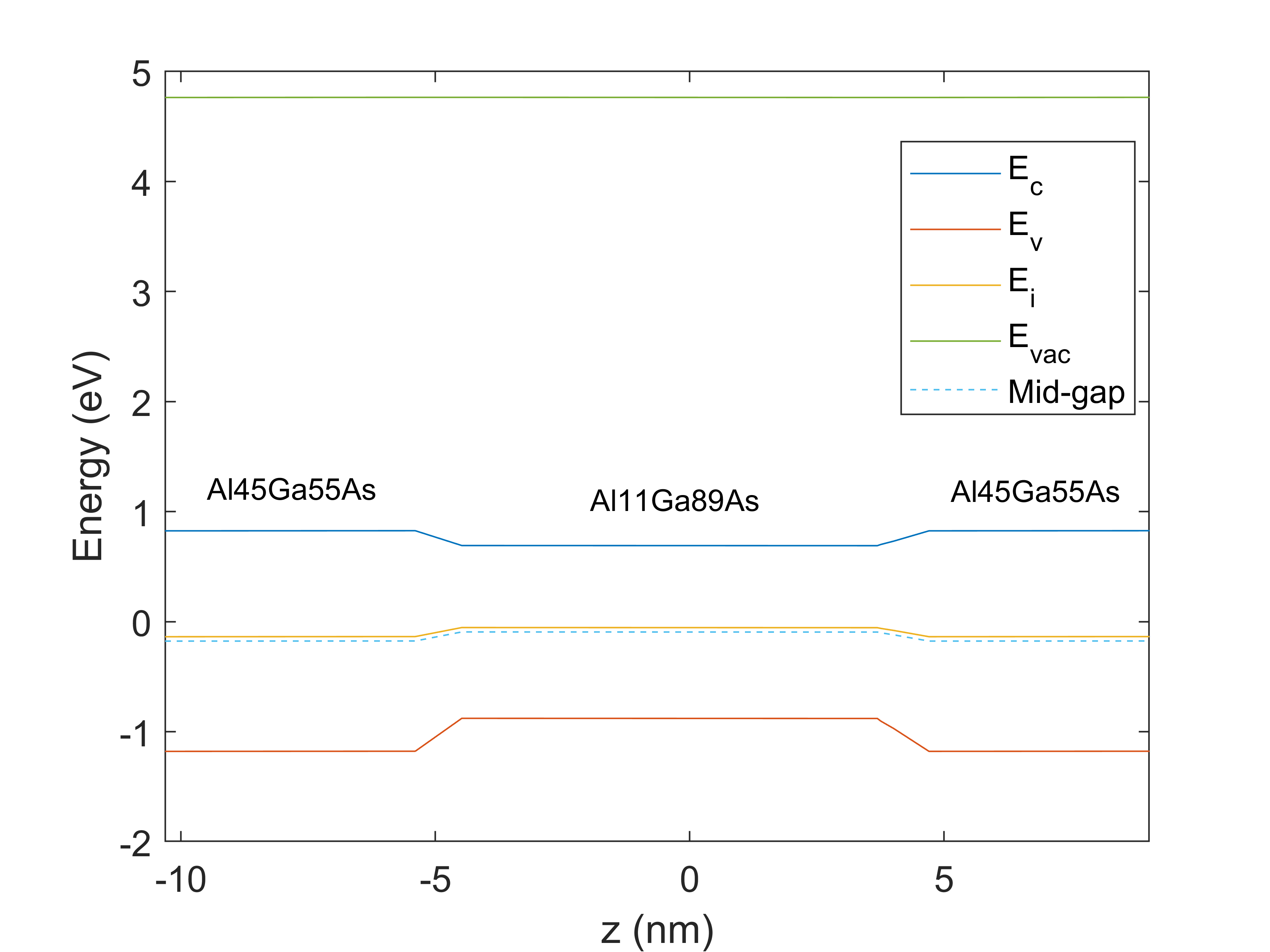
Following the link you sent me, I would expect the work function for my alloy to be calculated as a linear interpolation (W1*x+W2*(1-x)), as all the other electronic properties. The point is that, when I compute the band structure, I find different values of work function; values that I haven't managed to relate to the material properties set in the solver yet. For example, the following picture shows the calculated energy levels from CHARGE for a Al(0.45)Ga(0.55)As/Al(0.11)Ga(0.89)As quantum well, were I let the default bowing parameters; with default values W(GaAs)=4.83eV and W(AlAs)=4.97eV, I'd expect W(Al45)=4.8794eV and W(Al11)=4.8454eV. From the calculated energy levels, by doing Evac-Emidgap (as described here: https://optics.ansys.com/hc/en-us/articles/12126864836115-Understanding-band-offsets-in-heterostructures), I get W(Al45)=4.94eV and W(Al11)=4.8579eV.
If I substitute the quantum well material with simple GaAs, I retrieve the good value for its work function (4.83eV), while getting W(Al45)=4.885eV (closer to the expected value), as if the way it's calculated depends on the surrounding materials (but how?).
The fact that I don't know how these working functions are calculated, doesn't allow me to calibrate my band offsets by just changing, for instance, the work function of AlAs. If I try, I never find the ecpected values (N.B. I need to change it because the band offsets here are completely different from what expected from literature - confinement for electrons should by larger than the one for holes).
By comparing the two images, another thing that I can't understand is the shape of the quantum well barriers: why the solver doesn't retrieve step barriers when having an alloy as quantum well material (image 1) and it does when it's a simple semiconductor (image 2)? Simulation conditions are the same (mesh, BC, ...).
I'm trying to find a way to avoid to add new materials myself, since your built-in alloy "interpolator", with for instance the possibility of customizing the concentration variation, is incredibly useful and efficient (thanks for this feature!). If I don't solve this question I'm asking here, I think however it'll be my only possible solution.
Thanks again, best regards.
Lorenzo


