Ansys Learning Forum › Forums › Discuss Simulation › Photonics › Frequency Domain Field Profile Monitor on Plasmonic PA › Reply To: Frequency Domain Field Profile Monitor on Plasmonic PA
Hello Muhammad,
Thanks for your post.
Indeed your filed profile is quite coarse pixeled. At the top of my head, I would consider increasing the dz and dx meshing to get a more detailed electric field map. I would recommend to add a mesh element to your simulation region, so you can manually control the step size. Please refer to Mesh-override-Simulation-Object that explains in detail how to use the mesh element.
Also, you can refer to the Frequency-domain-Profile-and-Power-monitor-Simulation-object.
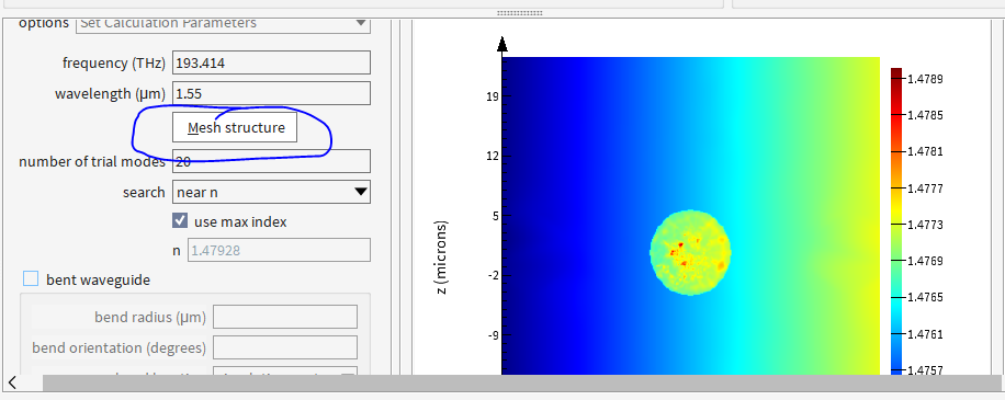
Regarding the material layer, I reckon that one reason that you cannot distinct is due to coarse mesh. I would recommend to check with the Refractive-index-monitor-Simulation-object (for FDTD) if you can see any materials difference as this is the appropriate tool to check the refractive index variation in your simulation region. Otherwise you can use the FDE or EME solver to check with "mesh structure" how your simulation design is structured, from refractive index perspective
I hope I helped. PLease let me know if you need further assistance with your model.
Kind regards
Dimitris


