Ansys Learning Forum › Forums › Discuss Simulation › Photonics › Error in CHARGE › Reply To: Error in CHARGE
November 16, 2023 at 8:45 am
 Alisa Bannaron
Subscriber
Hi Amrita,
Thank you for your reply!
I have checked the points you suggested.
- There are no warnings shown
- My design has top triangular electrodes where each triangle has some separation (currently 3 um, but it showed the same error at 20 nm as well). Intentionally I created the gap between electrodes since I wanted to avoid the charge overlap between them in an actual device so in the simulation I want to see what the sufficient gap is. I attached the screenshot of my design here. Could this gap be the cause of error in 2D Z-normal simulation?
*On alternative triangles the electrical I set in BC is like +/-
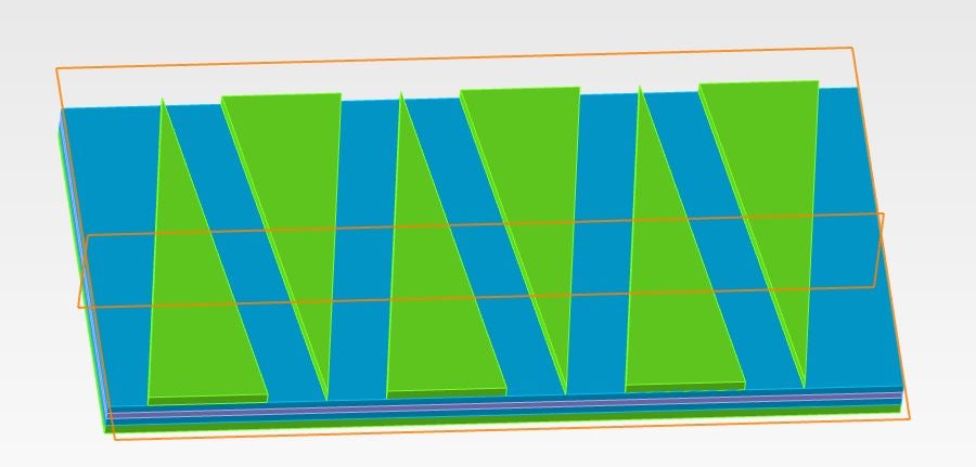
3. As you mentioned about the mesh, here is how I set up the global mesh constraint now. the size of the triangle (from the tip to the base) is 20 um and the thickness is 0.6 um. I have played with the max and min a bit, but the error remains.