Ansys Learning Forum › Forums › Discuss Simulation › Electronics › Modelling PCB warpage in Ansys Spaceclaim and Mechanical › Reply To: Modelling PCB warpage in Ansys Spaceclaim and Mechanical
June 29, 2021 at 9:23 am
Subscriber
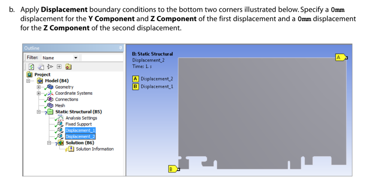
Thank you for the suggestion! The preliminary tests show reasonable results. Now I am hoping to figure out how would my boundary conditions affect the accuracy of my simulation. Currently, I have a thermal condition that heats the entire board from room temperature to 260 degrees Celcius (500 F), which is the maximum temperature in a reflow soldering oven. So far, I've attempted two setups: 1. Place a fixed support at the center node of the board 2. Place a fixed support at bottom right corner, a displacement [X: Free, Y: 0, Z: 0] at bottom left corner, and another displacement [X: Free, Y: Free, Z: 0] at top right corner (as shown in the image). This second approach is something I found in an Ansys presentation. One problem I found with the second approach is that I am interested in warpage out of plane, so a Z = 0 displacement condition would certainly affect my results. Whereas, the first approach would essentially be assuming that something is pinning down my board which doesn't exist in reality in a reflow oven. Please let me know if my thinking is correct, and also, any other boundary conditions that I could consider!


