TAGGED: pcb, simulation, siwave
-
-
October 5, 2020 at 4:13 am
Dracarys99
SubscriberI am trying to use ANSYS SIwave for EMI/EMC testing of my PCB. I have the following questions which don't seem to be covered in the tutorials: -
1) Suppose I am working with +5V, +12 V and +18 V on my board which are supplied through pin headers. And I have 2 components which use the +12 V say - a voltage regulator and a PWM IC VCC supply. Do I have to keep the pin header and regulator BOTH as a voltage source and PWM IC as a current source?
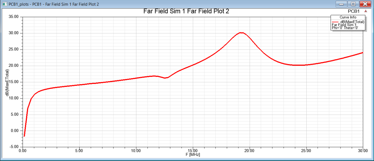
2) When I make a far-field computation using the Far Field simulation tool, it gives me several results. What is the Y axis representing in this plot?
October 8, 2020 at 4:36 amSubscriberI need this a bit urgently, it is for a project I'm working on so any points in the right direction would help too.nOctober 9, 2020 at 8:26 amSubscribernOctober 14, 2020 at 11:37 amSubscribernOctober 14, 2020 at 4:11 pmManny R
Ansys EmployeeHello! Thanks for your questions. Please see my answers below.n1.) It appears to me that you're trying to run a DCIR simulation and that being the case, your settings seem reasonable. PWM IC consumes power so you can define a current sink to it. We have complete end to end DCIR workflow videos right from reading the schematic of a board. Watch Part 1and Part 2- all the configuration steps are covered. These videos will give you a clear idea of where and how to define voltage sources and current sinks on a PCB before running a DCIR simulation in SIwave.n2.) At each frequency, SIwave plots the max value of Etotal. It is plotted in decibels since it distributes the points logarithmically allowing for a smaller set of values of Etotal and a smoother curve to be displayed on the graph. You can, however, set this to any appropriate Function such as mag or dB. To do this, navigate to the project manager window in Electronics Desktop and just double-click the report option. This operation will open the Reporter dialog. From here, you can select the Function of interest instead of dB.nOctober 14, 2020 at 4:20 pmAnsys EmployeeFinally, since you are doing a EMI/EMC testing of your PCB, you may want to consider doing DRCs in SIwave - use the EMI Scanner and the subsequent EMI Xplorer capabilities to identify areas of potential interference on PCB prior to simulation. With Xplorer you can further study the shades of gray in the violations. nOctober 27, 2020 at 7:46 pmSubscriberI'm using SIwave version 17.2, I don't see EMI Xplorer or EMI Scanner in this. I think I have to upgrade to the newer version for this. Also, could you explain with respect to the graph that I've posted here its meaning, that will help me realize if it is something totally wrong. I had thought that Far field results meant radiated emissions, and it may be that I'm wrong. So it would help if I were pointed in the right direction.nOctober 28, 2020 at 6:17 pmAnsys Employee1.) Yes, EMI Scanner and Xplorer capabilities are available in later versions of SIwave such as 2019 R2 and higher.n2.) To an extent you are right. Consider an example of a net transitioning from a layer through a via to a bottom layer and continuing along. Let's say the net is referencing power and ground planes respectively on the upper and lower layers and assume that caps are missing in this region. The caps here are supposed to ensure a continuous return path for the current. A far field simulation can give you a plot depicting a picture of the impact of plane resonance on the maximum radiated electric field. So, decoupling caps can be added to alleviate this radiated emissions issue - the caps can be added between power and ground planes. Adding these decoupling caps can shift the resonance and suppress the far field peaks and reduce the associated electric field. nViewing 7 reply threads- The topic ‘SIwave far field simulation results’ is closed to new replies.
Ansys Innovation Space Trending discussions
- How does Ansys Twin Builder implement different simulation steps for subcircuits
- Simulation of capacitor combining eddy currents with displacement currents
- Compute near field simulation with current
- Double-sided LIM external circuit error
- Ansys Resonance simulatioin error
- HFSS: Using Q3D to solve the DC point
Top Contributors
-
peteroznewman
 3139
3139 -
javat33489
 1007
1007 -
scabo
 918
918 -
Shyam Prasad V Atri
 858
858 -
adib.aktab999
792
Top Rated Tags
© 2025 Copyright ANSYS, Inc. All rights reserved.
Ansys does not support the usage of unauthorized Ansys software. Please visit www.ansys.com to obtain an official distribution.
-


The Ansys Learning Forum is a public forum. You are prohibited from providing (i) information that is confidential to You, your employer, or any third party, (ii) Personal Data or individually identifiable health information, (iii) any information that is U.S. Government Classified, Controlled Unclassified Information, International Traffic in Arms Regulators (ITAR) or Export Administration Regulators (EAR) controlled or otherwise have been determined by the United States Government or by a foreign government to require protection against unauthorized disclosure for reasons of national security, or (iv) topics or information restricted by the People's Republic of China data protection and privacy laws.