-
-
October 10, 2024 at 7:16 am
1906072
SubscriberHi everyone,
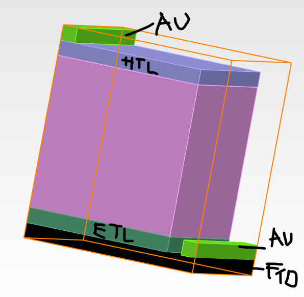
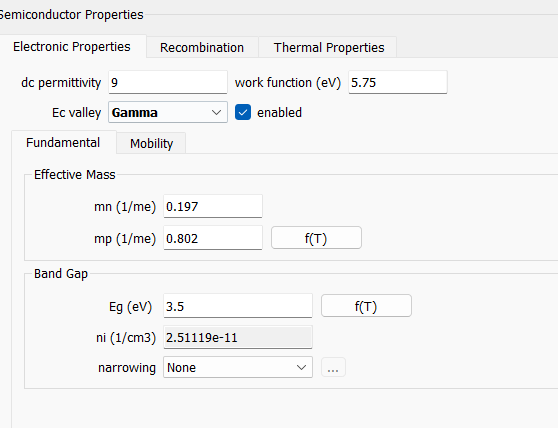
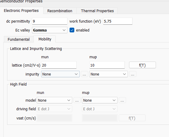
I’m simulating a perovskite solar cell with ZnO (ETL), MAPbICl₂ (absorber), and PEDOT(HTL). Instead of using FTO as a contact, I set it as a semiconductor with Au as the bottom contact to study the effects of FTO doping.However, I’m getting this error: "Semiconductor FTO is not correctly configured. Please verify material properties and configuration."
I’ve double-checked FTO properties from multiple papers, and they seem correct. The simulation works if I use FTO as a contact and remove the bottom Au contact layer.
Has anyone encountered this or can help with FTO configuration? I’ve attached my setup and FTO properties. Any advice would be appreciated!
Thanks!
-
October 10, 2024 at 4:45 pm
Guilin Sun
Ansys EmployeeThe error message says material and configuration are incorrect. Since you checked that the data is correct, it might mean some parameters are missing, or improper. I would suggest you to compare the material data with another well known and similar material.
In addition, it seems your version is quite old. Please upgrade to the newest version.
-
- You must be logged in to reply to this topic.


-
5649
-
1885
-
1403
-
1303
-
1021

© 2026 Copyright ANSYS, Inc. All rights reserved.


.png)


