-
-
September 9, 2024 at 7:27 am
ph23resch01002
SubscriberHi Sir/Madam,
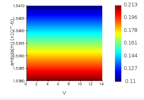
I am reproducing the work titled "Tunable all-dielectric metasurface for phase modulation of the reflected and transmitted light via permittivity tuning of indium tin oxide." I simulated the structure using Lumerical Charge and placed an ID monitor (Linear z) to obtain a plot showing the relationship between applied voltage and carrier concentration. Additionally, I used the NP attribute to convert the change in carrier concentration into a refractive index change. After simulating the unit cell, I obtained a plot that matches the results shown in the original paper. However, when I run the parameter sweep of applied voltage vs. transmission, I see no change, whereas in the original paper, there is a change in both the transmission coefficient and transmission phase. I am unsure where the issue lies.
While attempting to resolve this problem, I checked the NP attribute, but I am unable to control the Z and Z span. In the unit cell, I placed the charge monitor in two locations in Lumerical Charge to observe how the carrier concentration varies with applied voltage and, consequently, the refractive index. At one location, the Z and Z spans are 0.212 μm and 0.024 μm, while at the other, they are 0.391 μm and 0.31 μm. However, in the NP attribute, the Z and Z spans are fixed at 0 and 1 for both regions. Even if I attempt to change them, the Z span defaults back to 1 μm.
Can anyone guide me on this issue?
Kind regards,
BharathyThe attached first image is what I get and the below one is what is shown in the original paper.
-
September 10, 2024 at 5:37 pm
Guilin Sun
Ansys EmployeeFrom your description, it seems the applied voltage is not swept when you do the sweep for transmission simulation (FDTD). When you do the sweep, please select the sweep object to be the attribute, and only choose the voltage point to be the sweep parameter. You can visualize the attribute to check the max numbe of points.
In addition, the line monitor in CHARGE has only 1D result, which might not work in FDTD, as it needs the attribute to be 2D or 3D if you simulate transmission in 2D and 3D. A 1D change of the carriers does not change the device performance since it is so small. Please make sure the attribute is applied to the proper geometry as in the real device.
-
September 11, 2024 at 4:52 am
ph23resch01002
SubscriberHi Sir,
As you said, I have selected the sweep object to the attribute only, it seems like, the transmission amplitude changes very negligibly with respect to the applied voltage. That's why we are unable to see the difference. I have to check why it is changing only negligibly. If you can give any suggestions on this, it would be great.
Thank you,Kind regards,
Bharathy
-
September 11, 2024 at 3:10 pm
Guilin Sun
Ansys EmployeeHI Bharathy , what is the dimension of the attribute and what is the dimension of your transmission simulation? I suspect that the line monitor you use din CHARGE is not sufficient for FDTD simulation as mentioned in my previously reply.
Please give some screenshots of the simulations and device configuration.
-
- You must be logged in to reply to this topic.


-
5934
-
1906
-
1420
-
1306
-
1021

© 2026 Copyright ANSYS, Inc. All rights reserved.


