TAGGED: -waveguide, 3DFDTD
-
-
July 26, 2024 at 7:55 am
Rajat Kumar Sinha
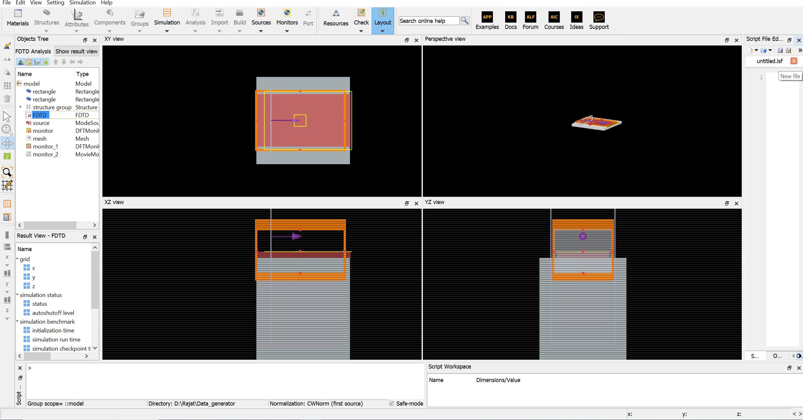
SubscriberI have designed a waveguide system with SiO2 substrate and waveguide layer of n=1.57 which is 300 nm thick(z span), 18 um wide(y span) and 30 um long (x span). My modal source launches TE fundamental mode(Ey dominated) along x axis at a wavelength of 632 nm. The FDTD region is x span= 30 um, y span=20um, z span=2 um(see image 1).
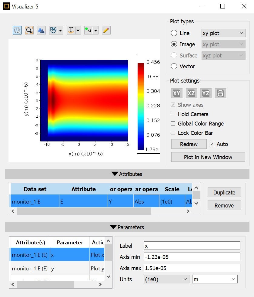
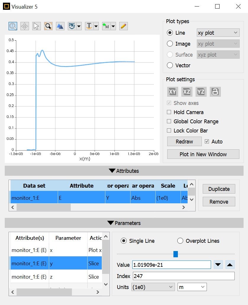
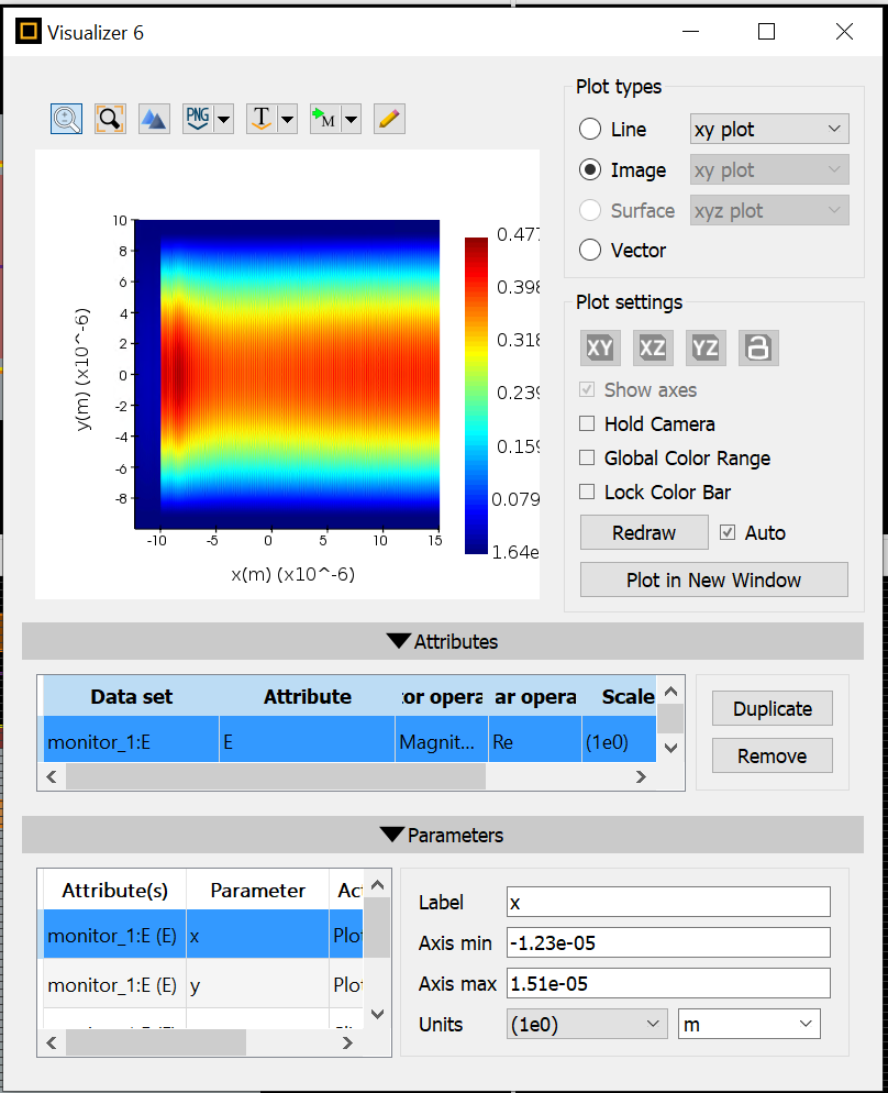
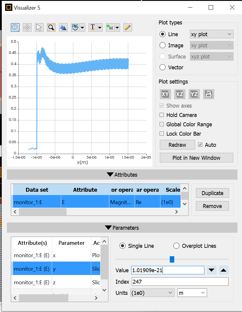
I am trying to measure the Electric field on top of the waveguide( at waveguide - air interface). My understanding is that electric field should exponatially decaying in x axis ( as it propagates) when I am trying to see the electric field profile in xy plane at top of the waveguide, I see wavy pattern near the source which dont make sense(at x=-8um in image 2). When I try to plot the same using line plot at y=0( centre of the waveguide) i could not only see wavy patterned near the source (at x=-8um in image 3) but also i see the abs value of electric field increasing after some distance( after x=-5um in image 3) which seems very counterintuitive.
I even tried changing the BC in the x direction from standard to stablized but similar problems occur.
any suggestion on how to rectify this mistake.
-
July 26, 2024 at 5:21 pm
Guilin Sun
Ansys EmployeeFirst, for the wavy feature, it might be related to source excitation which clips the mode field (please use log scale to check the mode profile), or the simulation span is short which cut the mode field profile.
Please increase the the lateral spans perpendicular to the propagation.
When the source profile is clipped it will cause diffraction.
When you plot the cut-line, make sure it is cut at the center of the profile.
You may try a smaller waveguide with shorter wavelength.
Ideally the mode should propagate very similar to theoretical prediction. Thus the problem is due to improper settings.
-
- The topic ‘Regarding Electric field on top of the waveguide’ is closed to new replies.


-
5809
-
1906
-
1420
-
1305
-
1021

© 2026 Copyright ANSYS, Inc. All rights reserved.

