-
-
March 13, 2024 at 3:58 am
weng jiaying
SubscriberI want to add 4 internal waveport to obtain parasitic parameters cased by external packaging of diodes.Here,i extend the metal anode to the interface between the epitaxial layer and the buffer layer, and equivalently set the epitaxial layer as GaAs material and the buffer layer as conductor material.
As this figure shown,the green layer is epitaxial layer and the orenge layer is buffer layer,the yellow layer is metal anode.
In order to obtain the S parameter of the parasitic parameter, I set a coxial waveport as shown.
But there is a problem when I run a simulation, and I ask for a help.
-
March 13, 2024 at 1:28 pm
dushyant.marathe
Ansys EmployeeHi Weng,
It seems that your model has internal wave ports. The error is appearinng becasue probably you do not have a PEC object defined on the internal waveports.
In HFSS, A wave port must have 'solve inside' objects on one side only. An internal wave port
would require a PEC object to be attached to and cover the opposite side before the solution can
proceed.I would suggest you to refer HFSS help PDF and look for "Automatic PEC Creation on Wave Ports"
This section discusses more about internal waveport and how to create a automated PEC backing object.
Thanks,
-
- The topic ‘
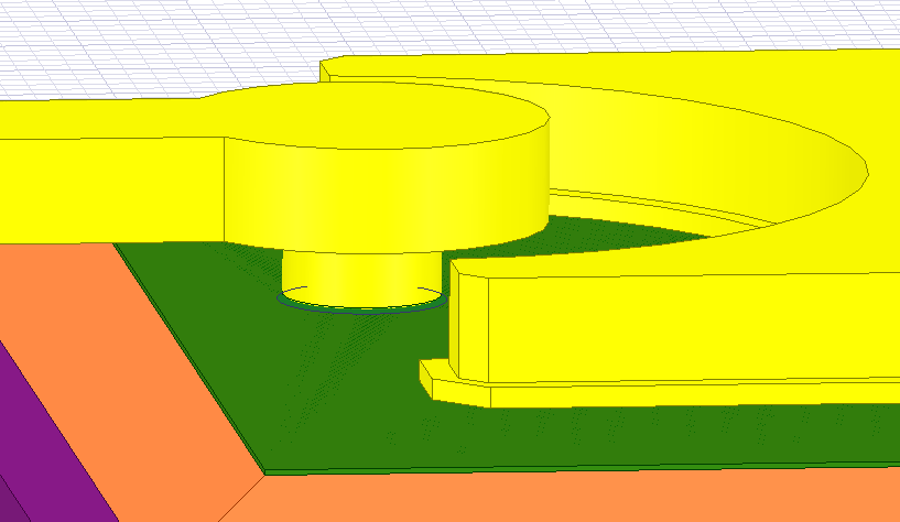
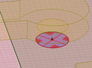
How to set a coaxial waveport for a Schottky diode 3-D model?’ is closed to new replies.
-
3492
-
1057
-
1051
-
965
-
942
© 2025 Copyright ANSYS, Inc. All rights reserved.