Ansys Learning Forum › Forums › Discuss Simulation › Photonics › Charge solver electrical contacts › Reply To: Charge solver electrical contacts
March 12, 2024 at 4:55 pm
Ansys Employee
Hi Nuaman,
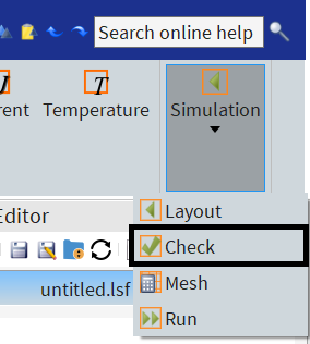
You should be able to directly apply contacts to a semiconductor, but the simulation region should have at least one other active semiconductor material for the solver to work. I applied voltage BC to a semiconductor and I can see it applied to that domain. Can you send a screenshot of the General and Geometry tabs of the contact BC? Which domain number is it? Can you visulalize that from the "simulation region"? Also after partitioning, when you click on "Check", do you see any error/warning messages?
Regards,
Amrita
