TAGGED: charge, current, electrical-contact
-
-
March 12, 2024 at 1:28 pm
-
March 12, 2024 at 4:55 pm
Amrita Pati
Ansys EmployeeHi Nuaman,
You should be able to directly apply contacts to a semiconductor, but the simulation region should have at least one other active semiconductor material for the solver to work. I applied voltage BC to a semiconductor and I can see it applied to that domain. Can you send a screenshot of the General and Geometry tabs of the contact BC? Which domain number is it? Can you visulalize that from the "simulation region"? Also after partitioning, when you click on "Check", do you see any error/warning messages?
Regards,
Amrita -
March 13, 2024 at 10:55 am
nuaman.m.kutty
SubscriberHi Amrita,
Thankyou for your reply!
I was double checking this simualtion that the results are true not not. The porject that I posted happened when I tried it for the second time, which means I already had results of the same LED stack with different compinations! However, it worked again when I started a new project from scratch! But the results (I-V curve) is slightly boosted with similar trend.Â
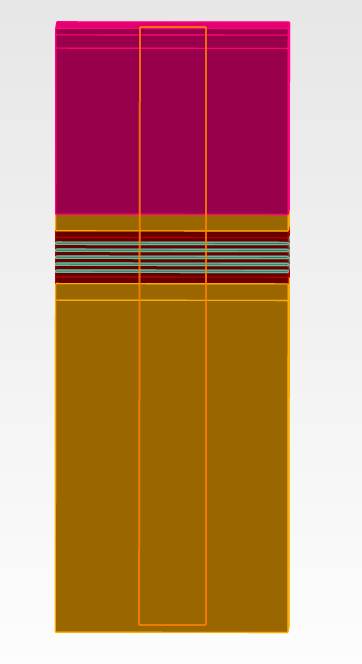
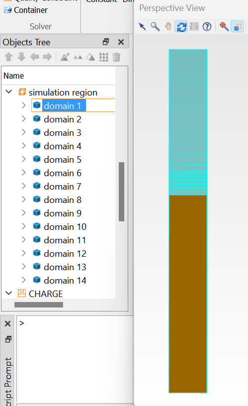
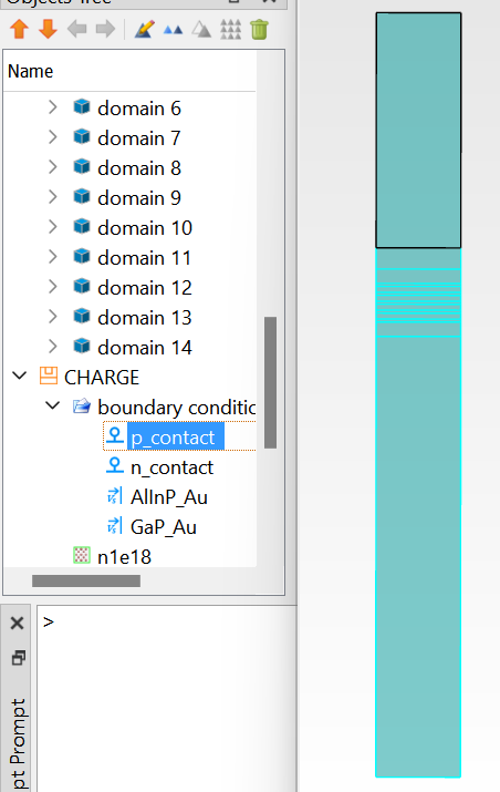
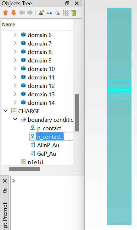
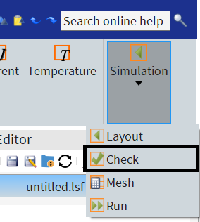
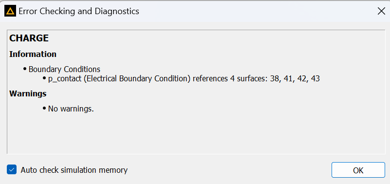
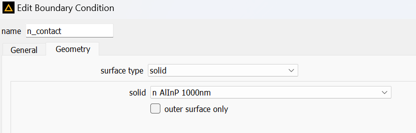
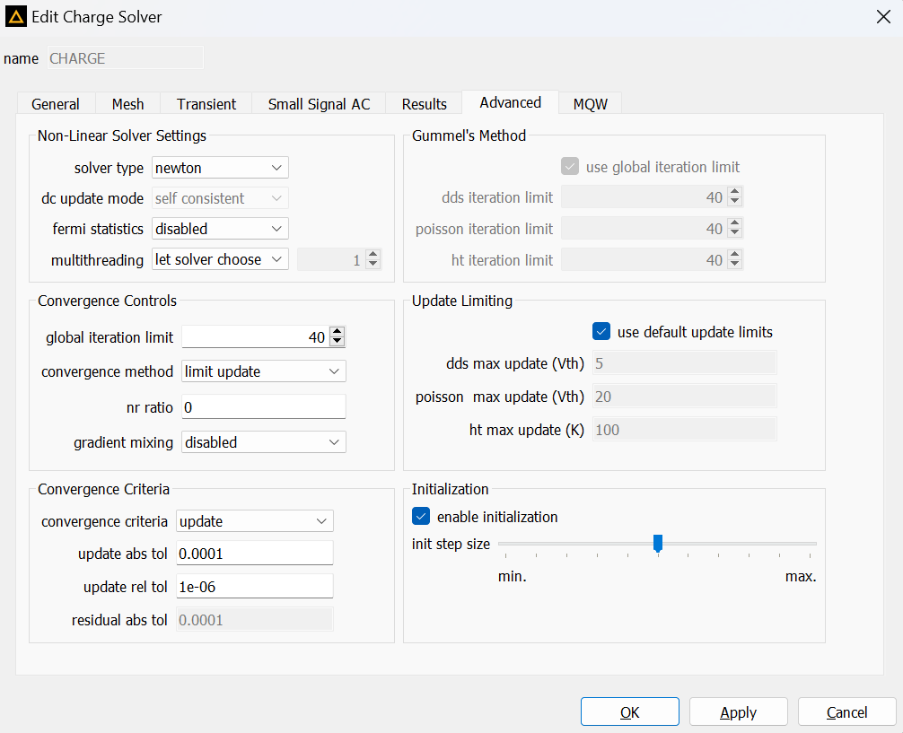
I have several confusions regarding the solver. How are these domains created? sometimes the domains are created as a single one if there are same material for geometries adjacent to each other, but now I noticed that the solver defined the domains as different ones for the same condition. Secondly, when the solver is not able to converege the results after many iterations, If i just go throgh all the objects/ domains/ BC, and then runs it, sometimes it runs, or if i just close the project and reopen it again then >layout>partition>run, it runs!
So I doubt that I need to understand how things work properly or the solver is not running properly!
Will it be possible to have a zoom meet or any live sesseion to clarify more about the CHARGE solver? It would be great if you could makei t!
Regards,
Nuaman -
March 13, 2024 at 6:07 pm
Amrita Pati
Ansys EmployeeHi Nuaman,
I probably won't be able to make it today. Plus, there are some policy restrictions on the ALF side as well. But let me get back to you on this by tomorrow.
Regards,
Amrita -
March 14, 2024 at 7:14 pm
Amrita Pati
Ansys EmployeeHi Nuaman,
I talked about this with my team. Unfortunately, we are not allowed to setup meeting/exchange files with ALF users due to some policy restrictions. If you would like to setup a meeting, I will recommend reaching out to your Ansys Sales Representative. They will know how to connect you with the right person.
In the mean time, the solver behaviour that you explain is not expected. I will look into this and get back to you here.
Regards,
Amrita -
March 19, 2024 at 1:06 pm
nuaman.m.kutty
SubscriberHi Amrita,
As mentioned before, I am experiencing the same. when I started a new project, the n contact is not recognized.
here are the screen shots.The two GaP layes are cosidered together as a single domain as well as P contact even thought I have only selected the last layer. Simillarly for the N side, the 2 AlInP layers are together a single domain but it is not recognized as the N contcat.Â
-
March 19, 2024 at 5:29 pm
Amrita Pati
Ansys EmployeeHi Nuaman,
I don't really see why the contact is not recognized. I ran multiple simulations, I haven't checked the validity of the results yet but the contact is recognized in each case and the simulation runs successfully. After you partition, can you go through the domains one after the other and see that each domain has the right material assigned to it? Which domain number is the n-AlInP 1000 nm?Â
Regards,
Amrita -
March 20, 2024 at 12:25 pm
nuaman.m.kutty
SubscriberHi Amrita,
Finally, I was successfully able to do it from scratch. What I think the problem was, while adding the material I did 2 things, 1- Before adding the ternarry alloys, I added all the related primary materials (like AlN and GaN for AlGaN). 2- While adding the ternarry alloys, I was going with the "create semi" option, which wasn't working and when I added with "create new" option, it worked.
worth to mention that when I added a gold contacts for the device with ternary alloys added in "create semi" option it was running.
Also I would like to mention that still at some point this happened that it shows error mentioning couldn't converege the results after xxx iteration, and when I just go back to layout mode > partition > run, it works! I don't know what happened.Â
Other things that I noticed is previously the AlInP layers in the n side were considered as a single domain (Domain 1). Simillary the GaP on the p side. But now the AlInP and GaP layers are considered as seperate domains. Also the order or the position of the layers in the geometry tab is considered when creating the domain (if a layer is not positioned according to the order of the device stack, that layer will be having a domain number corresponding to the order of layers in the geometry tab). -
March 20, 2024 at 2:40 pm
nuaman.m.kutty
SubscriberHi Amritha,
I would like to know if the order of the domains has any role in the results. I want to add a DBR consisting of 30 pairs in between the n AlInP 1000nm and n AlInP 50nm layers of the previous design. When I made the structure (I did duplicated the layer and then changed the parameters like geometry and material accordingly), after the partiotion the domains are completely random ordered and I am obeserving a huge drift in the expected results. Also I would like to mention that the simulation could only sweep until 2V and then it couldn't converge. Once I closed and reopened the file, then layout > partition > run, it works until 3V
Regards,
Nuaman -
March 20, 2024 at 7:56 pm
Amrita Pati
Ansys EmployeeHi Nuaman,
I am glad to know that you were able to solve the first issue. I am not really an expert on CHARGE, I work more on the photonic side, but allow me some time to discuss these issues with R&D. I believe they will be able to provide more useful insights, I will get back to you then.
Regards,
Amrita
-
- The topic ‘Charge solver electrical contacts’ is closed to new replies.
- Import material .txt file with script
- Errors Running Ring Modulator Example on Cluster
- Absorption cross-section of AuNR excited by prism-based TIR
- How to measure transmission coefficients on a given plane .
- TE Polarization Fraction + Waveguide TE/TM Fraction
- Edge Coupler EME Example Issue
- Lumerical Python API Topology Optimization Error 2025 R1
- 2D inverse design grating coupler
- FDE : Simulation waveguides with electrodes
- Loss of lithium niobate phase modulator
-
2342
-
925
-
599
-
591
-
527
© 2025 Copyright ANSYS, Inc. All rights reserved.