-
-
March 6, 2024 at 10:43 am
Lorenzo Lazzari
SubscriberHello,
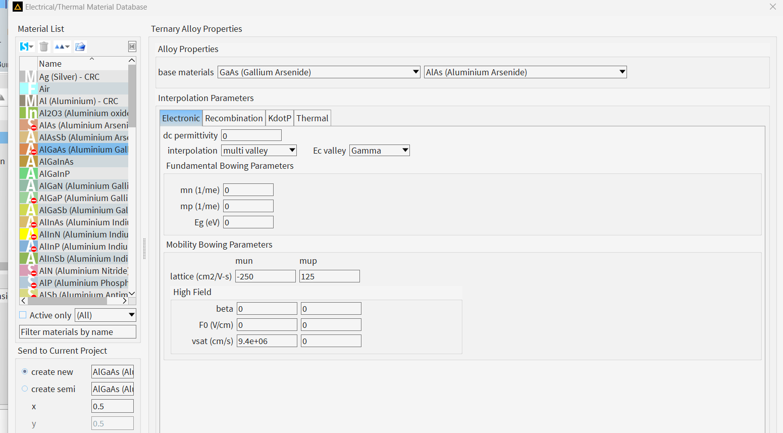
I'm trying to simulate an AlGaAs diode laser with Lumerical CHARGE + MODE. I'd like to retrieve the electronic properties of a given AlGaAs alloy, as they are automatically interpolated by Lumerical (to be coherent with the results of the electrical simulation).
The first solution I guess would be to get all the properties of GaAs and AlAs, the bowing parameters and manually retrieve the alloy properties by following https://optics.ansys.com/hc/en-us/articles/360034398494-Alloy-material-model-properties . Is there a faster way? Since these properties are already calculated by the software, I imagine that they are stored somewhere, and maybe they can be directly obtained.
Thanks in advance! Have a nice day.
Lorenzo
-
March 7, 2024 at 6:10 pm
-
March 7, 2024 at 6:12 pm
Guilin Sun
Ansys EmployeeCHARGE solvers gives charge and electric fields as output. No other results are given:
https://optics.ansys.com/hc/en-us/articles/360034917693-CHARGE-solver-introduction
-
March 8, 2024 at 10:25 am
Lorenzo Lazzari
SubscriberThanks for your answer.
The point is that, when considering an alloy A(x)B(1-x), I user-set (some) bowing parameters (C) and the concentration x, and then the software interpolates the electronic/thermal properties (P, eventually present in the database) of the two species composing the alloy by using: P[A(x)B(1-x)]=x*P(A)+(1-x)*P(B)+x*(1-x)*C, as detailed in the reference I gave in the original post.
Now, to retrieve the interpolated properties I'm currently manually getting the properties of interest (P(A), P(B)) from the database and perform the interpolation myself. I was wondering if there is an easier way to get those interpolated properties somewhere, since they are already automatically calculated by Lumerical, but as you were mentioning they don't appear in the simulation results.
Hope it's clearer, thanks again.
-
March 8, 2024 at 4:21 pm
Guilin Sun
Ansys EmployeeI believe internally the solver calculates the material properties of the alloy with the method you mentioned.
https://optics.ansys.com/hc/en-us/articles/360034398494-Alloy-material-model-properties
https://optics.ansys.com/hc/en-us/articles/360034919153-Setting-the-alloy-mole-fraction
you can add material properties:
https://optics.ansys.com/hc/en-us/articles/360034924933-addmaterialproperties-Script-command
more semiconductor properties:
https://optics.ansys.com/hc/en-us/articles/360034919113-Semiconductor-Material-Model-Properties
However I did not find any script to get them directly. You may try to use "get" and see if it works.
?getnamed("materials::AlGaAs (Aluminium Gallium Arsenide)::AlGaAs (Aluminium Gallium Arsenide)");
gives you all the names of the material properties.
?getnamed("materials::AlGaAs (Aluminium Gallium Arsenide)::AlGaAs (Aluminium Gallium Arsenide)","electronic.single.mp.bowing");
result:
0It should be what you input for the material.
-
March 22, 2024 at 8:06 am
Lorenzo Lazzari
SubscriberHello, thanks for your answer. It does work and correctly returns the bowing parameters, but it doesn't return the interpolated properties for a given alloy concentration x - that I still have to interpolate manually. This has become a problem when dealing with band offsets: as suggested here -> https://optics.ansys.com/hc/en-us/articles/12126864836115-Understanding-band-offsets-in-heterostructures , to calibrate band offsets to literature values one solution is to change one of the work functions of the two materials forming the heterojunction accordingly. The problem is that I don't understand how Lumerical computes the work function for an alloy: results retrieved from simulated band structures differ from what I could expect from a linear interpolation (W1*x+W2*(1-x)), hence I don't know how to properly calibrate the work function. Can you help me? I already verified that with normal semiconductors everything works fine.
Thanks in advance.
P.S. I could start a new post called "Work function for alloy materials" if you consider it's more useful.
-
March 26, 2024 at 5:40 pm
Guilin Sun
Ansys EmployeeHi Lorenzo, sorry to reply you late as I was waiting for a colleague's feedback.
As mentioned before, alloy can be formed from semiconductor materials and the properties are calcualted based on https://optics.ansys.com/hc/en-us/articles/360034398494-Alloy-material-model-properties
You can also add a new semiconductor material ("create new") with your calculated parameters.
-
March 27, 2024 at 3:50 pm
Lorenzo Lazzari
SubscriberHello, thanks Guilin for your answer.
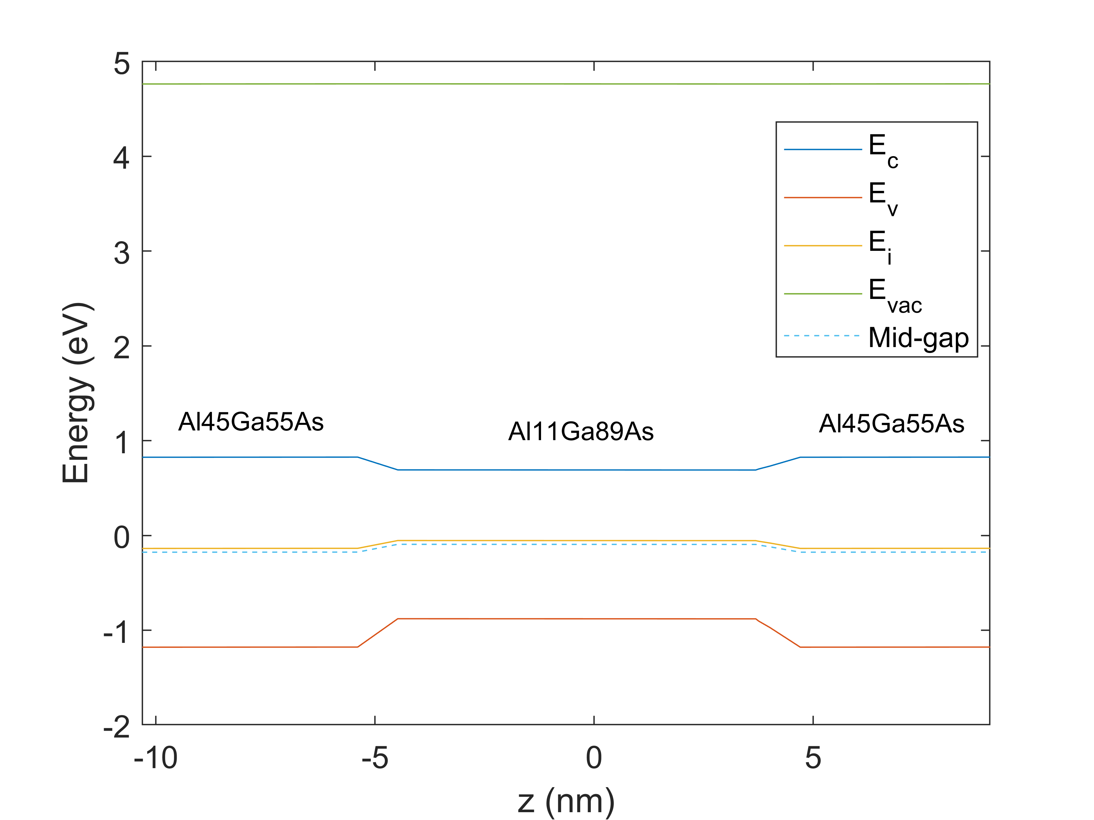
Following the link you sent me, I would expect the work function for my alloy to be calculated as a linear interpolation (W1*x+W2*(1-x)), as all the other electronic properties. The point is that, when I compute the band structure, I find different values of work function; values that I haven't managed to relate to the material properties set in the solver yet. For example, the following picture shows the calculated energy levels from CHARGE for a Al(0.45)Ga(0.55)As/Al(0.11)Ga(0.89)As quantum well, were I let the default bowing parameters; with default values W(GaAs)=4.83eV and W(AlAs)=4.97eV, I'd expect W(Al45)=4.8794eV and W(Al11)=4.8454eV. From the calculated energy levels, by doing Evac-Emidgap (as described here: https://optics.ansys.com/hc/en-us/articles/12126864836115-Understanding-band-offsets-in-heterostructures), I get W(Al45)=4.94eV and W(Al11)=4.8579eV.
If I substitute the quantum well material with simple GaAs, I retrieve the good value for its work function (4.83eV), while getting W(Al45)=4.885eV (closer to the expected value), as if the way it's calculated depends on the surrounding materials (but how?).
The fact that I don't know how these working functions are calculated, doesn't allow me to calibrate my band offsets by just changing, for instance, the work function of AlAs. If I try, I never find the ecpected values (N.B. I need to change it because the band offsets here are completely different from what expected from literature - confinement for electrons should by larger than the one for holes).
By comparing the two images, another thing that I can't understand is the shape of the quantum well barriers: why the solver doesn't retrieve step barriers when having an alloy as quantum well material (image 1) and it does when it's a simple semiconductor (image 2)? Simulation conditions are the same (mesh, BC, ...).
I'm trying to find a way to avoid to add new materials myself, since your built-in alloy "interpolator", with for instance the possibility of customizing the concentration variation, is incredibly useful and efficient (thanks for this feature!). If I don't solve this question I'm asking here, I think however it'll be my only possible solution.
Thanks again, best regards.
Lorenzo
-
March 27, 2024 at 4:24 pm
Guilin Sun
Ansys EmployeeI guess when we reach quatum well, it might be a little different https://optics.ansys.com/hc/en-us/articles/360034926533-mqwgain-Script-command
I am not sure what exactly the internal interpolation is. You can setup a new semiconductor, and set the parameters from your own calculation.
-
March 27, 2024 at 4:47 pm
Lorenzo Lazzari
SubscriberI'll try to do like this then. Thanks for your help! Best regards,
Lorenzo
-
- The topic ‘Extract interpolated properties of an alloy material in CHARGE’ is closed to new replies.


-
5649
-
1885
-
1404
-
1303
-
1021

© 2026 Copyright ANSYS, Inc. All rights reserved.


