-
-
February 20, 2024 at 1:32 pm
Jordi Lopez Leyva
SubscriberI'm simulating a Photonic crystal in FDTD, where light should form a pattern similar to a grating (show in figure). I import a calculated optical generation into CHARGE. However, when I try simulate the carrier generation in CHARGE, I don't see the grating formation. Instead, carriers seem to be smoohted across the entire material instead of forming a grating. How can I ensure a grating is formed in CHARGE?
My simulation is with GaAs transient isothermal, 1000fs max steps (200ps steps) for 10ps simulation time with electrical boundary condition transient. Optical generation is on for only 100fs. I removed all recombination from the GaAs electrical material.
Optical generation:Â
initial E field:
Â
initial carrier generation (bottom is clipped through the middle, the top one is the volume plot showing the surface):
Â
-
February 22, 2024 at 5:30 pm
Jordi Lopez Leyva
SubscriberI figured out the issue was the mesh order. I copied my structure from FDTD, but mesh orders in FDTD depend also on refractive index. But in CHARGE this needs to be set manually.
-
- The topic ‘
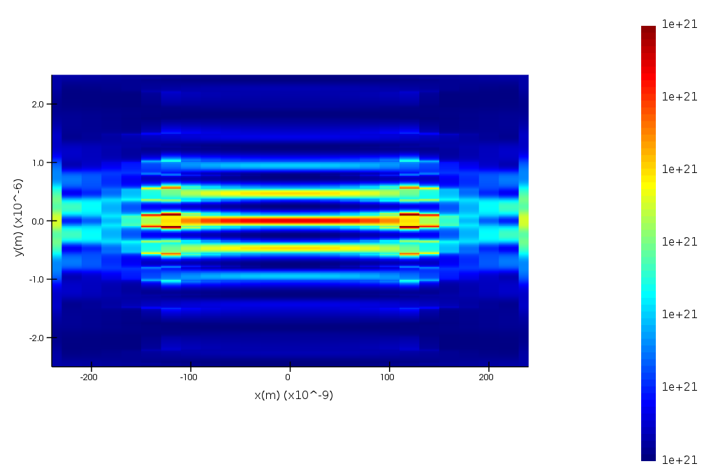
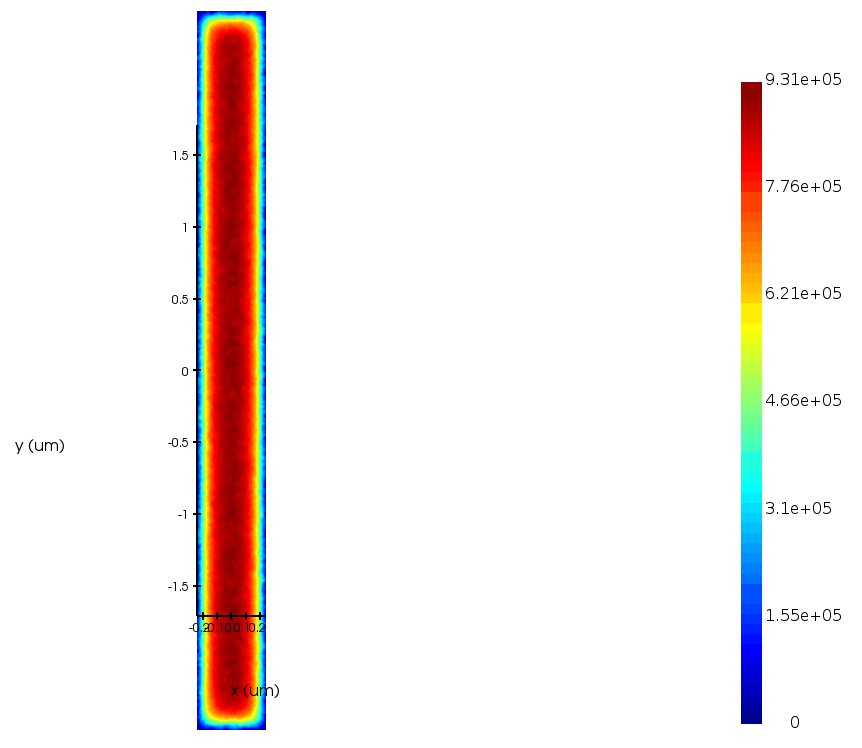
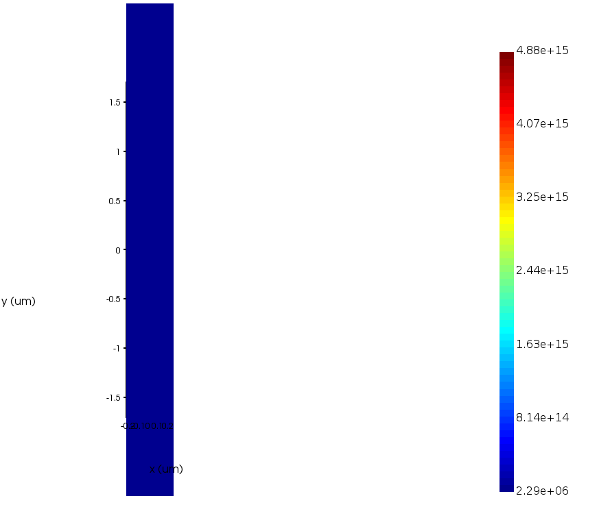
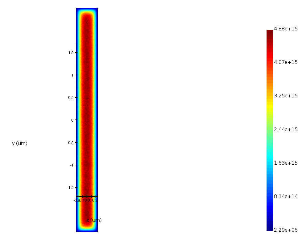
CHARGE optical generation pattern not maintained’ is closed to new replies.
- Difference between answers in version 2024 and 2017 lumerical mode solution
- Errors Running Ring Modulator Example on Cluster
- Import material .txt file with script
- Trapezoidal ring
- Help for qINTERCONNECT
- Absorption cross-section of AuNR excited by prism-based TIR
- Issues with getting result from interconnent analysis script
- How to measure transmission coefficients on a given plane .
- Topology Optimization Error
- Edge Coupler EME Example Issue
-
1882
-
802
-
599
-
591
-
366
© 2025 Copyright ANSYS, Inc. All rights reserved.