Dear Kawshik,
In the graphene material from the material database, you can define the scattering rate, the chemical potential and the temperature as shown below:
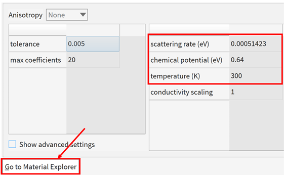
Did you use the default values or did you defined them to correspond to the correct conductivity for your frequency range?
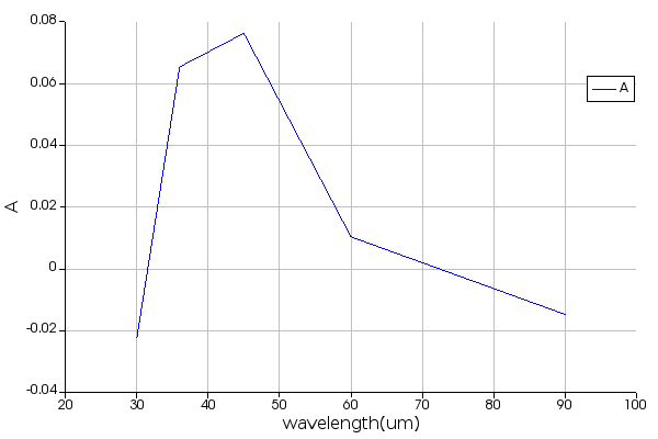
If you click on the “Go to Material Explorer” button shown above, you will see the conductivity vs wavelength for the graphene material. You need to define the above parameters to have the correct conductivity values for the desired wavelengths. For example, the default scattering rate and chemical potential values will give you the following conductivity in the wavelength range used in your simulation:
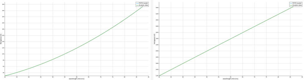
If you change the values to the ones shown in Figure 1 of Graphene surface conductivity material model – Ansys Optics for broadband graphene conductivity, the conductivity in the wavelength range used in your simulation will now be the following:
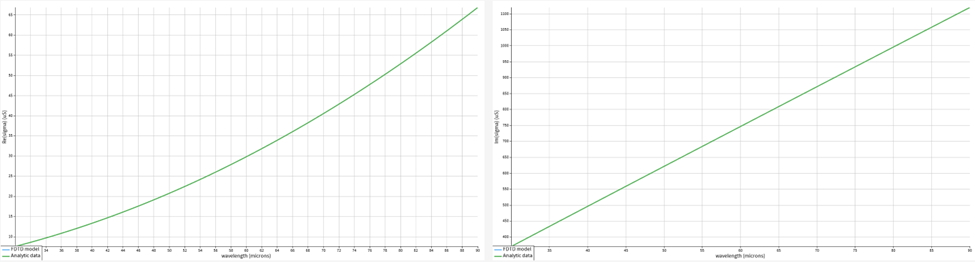
Hence, you need to be sure that the conductivity used in the simulation corresponds to the one that you are trying to simulate.
In the material explorer you should also check that the rest of the materials also have the correct values in the wavelength range of interest. Some of the materials in the material library might have limited data in other frequency ranges (optical, NIR wavelengths). In this case you will need to specify the correct values for these materials.
Concerning the setup of the simulation, I do not see anything wrong from the image that you shared. Do you have PML or periodic boundary conditions?
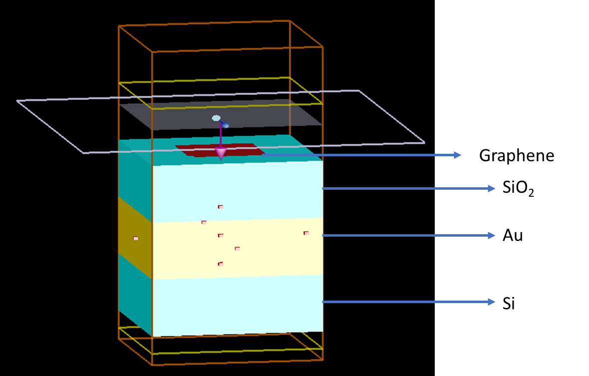
In any case the structure should extend through the boundaries as shown below:
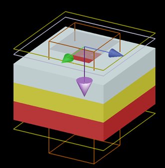
For example, if your FDTD in x and y axis extends from -10um to 10um, you need to make the Si, Au and SiO2 layers larger (e.g. from -12um to 12um).
Best regards,
Afroditi