Ansys Learning Forum › Forums › Discuss Simulation › Photonics › Help regarding the simulation domain , monitor dimensions › Reply To: Help regarding the simulation domain , monitor dimensions
 pnair
pnair
Hello,
Thank you for the reply.But, I am not clear about the FDTD simulation span and why the output results are varying for different simulation volume. I have SIC thin film of thickness 340nm. So, I have assumed it is infinitely long in x&y directions. Then I have selected a FDTD Simulation region of 3x3x1um on my thin film which is 8x8x0.34um. Then I place a DFT monitor of 10x10x 0.4 This means that i have placed a DFT monitor at a height of 0.4um from the surface of my simulation region..please see the attached screen shots of the geometry of the structure.
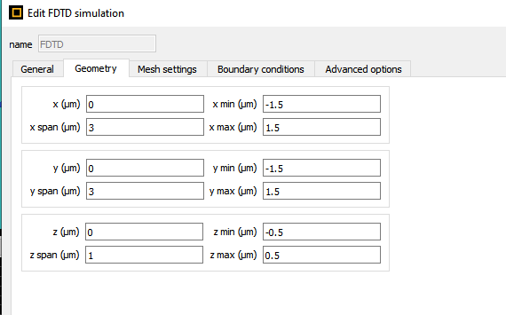
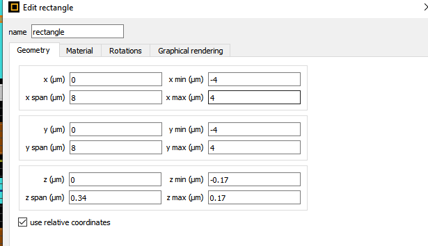
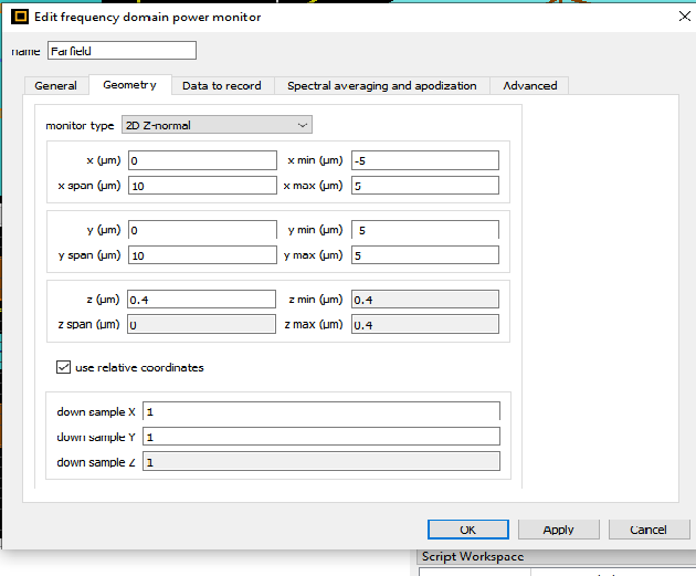
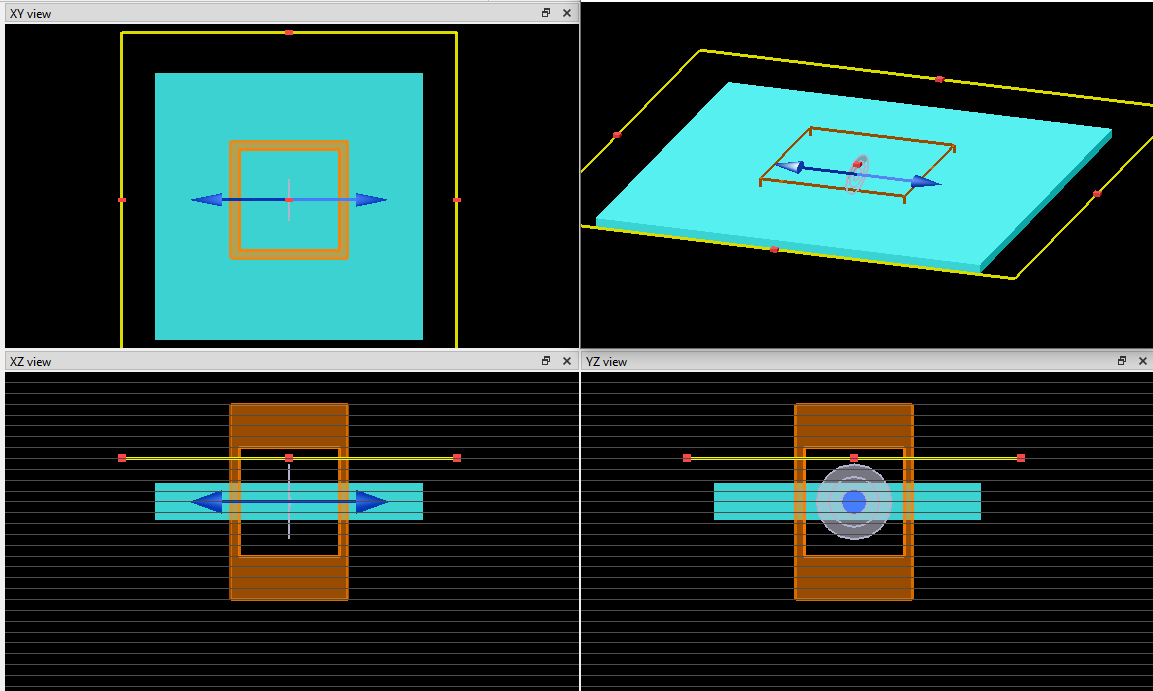
This is how I have set up the simulation window and monitors. But, the issue is that If I am changing the simulation volume, the the farfield emission pattern is also changing. Please suggest if there is any way to solve this problem.
