TAGGED: e-field, h-field-plot, plasmonics
-
-
January 29, 2024 at 10:47 am
Muhammad Irfan
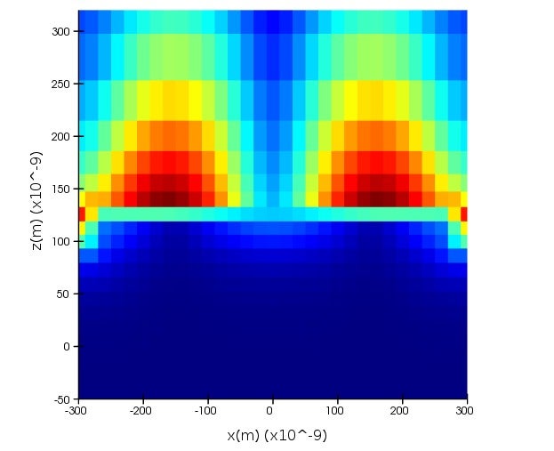
SubscriberI am trying to simulate a Plasmonic Perfect Absorber using Lumerical FDTD and everything is fine with plotting result. But when I try to get Frequency Domain Field Profile Monitor results for E-field and H-Field confinements (I am using separate monitors both each), the results seems distorted and pixelated. I have refined mesh and decreased yee-cell size to 0.1 nm, but it does not seem to have any affect on the output monitor field profile due to some unknown reason. I checked published research paper that used Lumerical and designed Plasmonic PAs and I noticed that their results are so fine and tuned. Also, I am unable to see any material layer distinction in the Frequency Domain Field Profile Monitor output. Attached is the result for ready reference.
-
January 30, 2024 at 10:17 am
Dimitris Polyzos
Ansys EmployeeHello Muhammad,
Thanks for your post.
Indeed your filed profile is quite coarse pixeled. At the top of my head, I would consider increasing the dz and dx meshing to get a more detailed electric field map. I would recommend to add a mesh element to your simulation region, so you can manually control the step size. Please refer to Mesh-override-Simulation-Object that explains in detail how to use the mesh element.
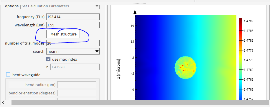
Also, you can refer to the Frequency-domain-Profile-and-Power-monitor-Simulation-object.Regarding the material layer, I reckon that one reason that you cannot distinct is due to coarse mesh. I would recommend to check with the Refractive-index-monitor-Simulation-object (for FDTD) if you can see any materials difference as this is the appropriate tool to check the refractive index variation in your simulation region. Otherwise you can use the FDE or EME solver to check with "mesh structure" how your simulation design is structured, from refractive index perspective
I hope I helped. PLease let me know if you need further assistance with your model.
Kind regards
Dimitris
-
January 31, 2024 at 7:35 am
Muhammad Irfan
SubscriberThank you for your detailed reply. I made the changes in dx and dz with mesh override settings and results have been greatly improved. But Still I am unable to make material distinction in the E-field confinement window. Is it because layers are too thin? Please note that I am using layers of thickness 0.345nm and 4nm in the design. Also, please guide how to keep field profile intensity bar between 0-1 range, in my case it shoots off to 29 high and low at 0.0912. When I manually adjust the value, the intensity of colors deteriorates.
-
January 31, 2024 at 9:57 am
Dimitris Polyzos
Ansys EmployeeHello Muhammad,
I reckon you are correct regarding the material distinction. If your override mesh is at the scale of 1 nm and as I can see the thickness you are using is in the order of 0.345 nm then you will not be able to see any difference in the material. Even if you decrease your mesh to 0.05 nm I believe that you are reaching to a limitation point of meshing. You can use the scale factor instead, however it will be difficult to distinguish the material structure for such tiny thickness.
A lot of information regarding the colorbar limits you can read this article:d Understanding frequency domain CW normalization. The unity 1 value you want to obtain in your colorbar, is normalized as the peak amplitude of the injected E-field which is enhanced in dielectric, however I reckon that your field components will be complex.
Please refer to Units-and-normalization-conventions-in-Lumerical-solvers for more information regarding the normalization.
I hope I helped. Please feel free to contact me for further information.
Kind regards
Dimitris
-
February 3, 2024 at 9:29 pm
Muhammad Irfan
SubscriberThank you for helping out in this matter. The issue has been resolved.
-
- The topic ‘Frequency Domain Field Profile Monitor on Plasmonic PA’ is closed to new replies.


-
5849
-
1906
-
1420
-
1305
-
1021

© 2026 Copyright ANSYS, Inc. All rights reserved.


