TAGGED: -Photonic-crystal, fdtd, lumerical
-
-
November 8, 2023 at 2:48 pm
Jordi Lopez Leyva
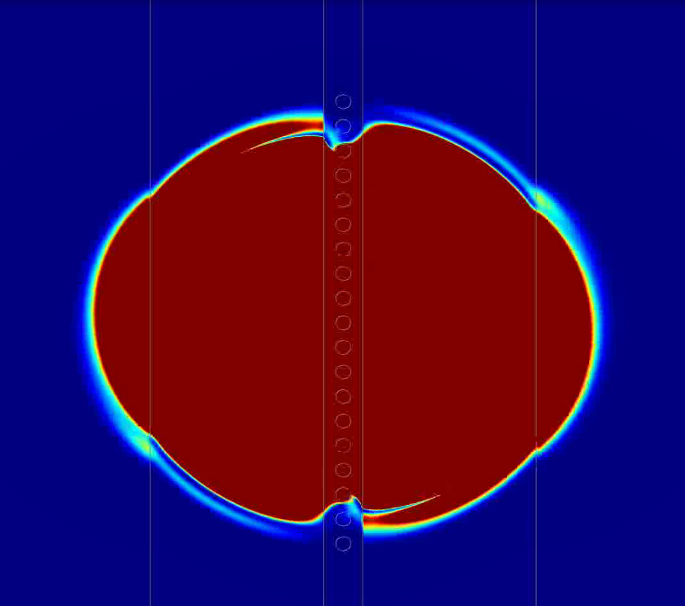
SubscriberI'm trying to simulate a 1D photonic crystal nanobeam of GaAs with pockels Chi2 effect. I'm doing so by implementing 2 dipole sources at the center. However, the movie shows no light is guided for high powers of the dipoles. For low dipole power I don't have this issue and light is perfectly guided.
I'm using 2 electric dipole source in FDTD, with total amplitude ~ 2e-24 and power ~2mW. I obtain power via dipolepower command. My material is GaAs nanobeam with Chi2, with air holes, and surrounded by SiO2 and a polymer of n = 1.6. I'm using standard PML boundaries and high mesh density.
Questions I have
- Am I calculating the power correctly?
- Do I need to change boundary conditions?
- How can I fix the simulation instability?
For reference, here's a snapshot of the movie:
-
November 23, 2023 at 1:18 am
Dev
Ansys EmployeeHello,
Please try not to post duplicated post in another Forum.
You can refer the optical forum post response: 3D FDTD simulation with 1mW dipole and nonlinear chi2 material not stable (ansys.com)
Thanks and regards
Devika
-
- The topic ‘Lumerical 3D FDTD simulation for Chi2 photonic crystal not guided’ is closed to new replies.


-
5664
-
1890
-
1419
-
1304
-
1021

© 2026 Copyright ANSYS, Inc. All rights reserved.


