-
-
February 27, 2023 at 8:25 am
Haiquan
SubscriberHello
I am facing some issues during trace mapping:
1/ When I import the tgz file in SpaceClaim, I found that there is no solid 3D. The ECAD engineer told me that
there is no 3D geometry in tgz file (I am surprised). What setting should they do in order to include the 3D in tgz? (They are using Zuken)2/ Based on the reason above, I tried to import only one solid body of PCB with stp format, is it OK if importing a stp 3D?
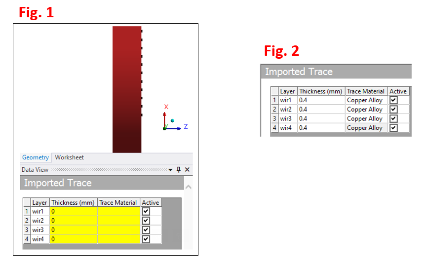
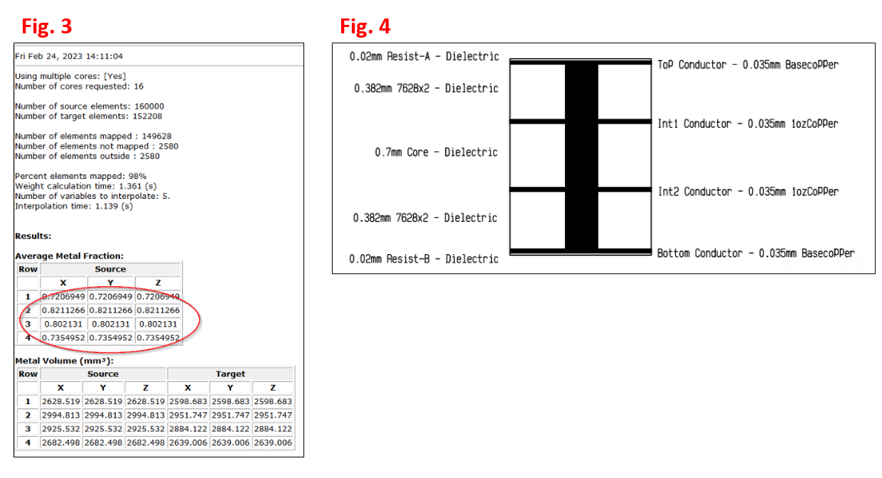
3/ After import the trace tgz file, ANSYS can identify 4 layers but with 0mm thickness as shown in Fig. 1, I input the thickness manually shown in Fig. 2 (total PCB thickness 1.6mm). I also generate 4 elements through the thickness
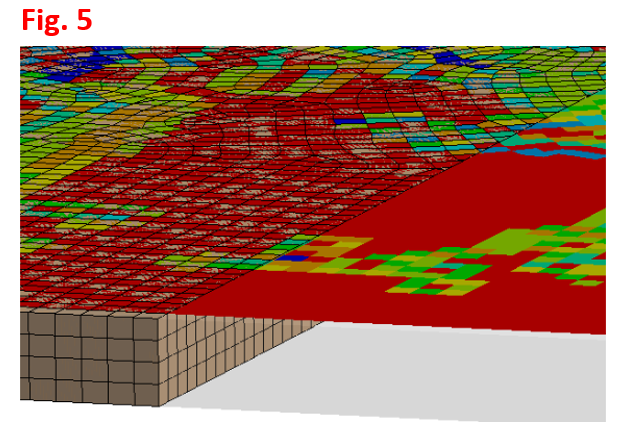
4/ After mapping, it seems not correct, the metal fraction is nearly 1 as shown in Fig. 3, it seems I lost the dielectric layers, the PCB stack up information is shown in Fig. 4. I made a section in the PCB as shown in Fig. 5. How should I build the 3D model based on this stack up information?
5/ In my understanding, the tgz should include 7 layers of the PCB stack up(ignore the solder mask layers Resist A and B), is it correct?
Thank you very much for your feedback
-
February 27, 2023 at 10:14 am
ErKo
Ansys EmployeeHi
I would suggest to create a support request as we might need to see the model and try and import the trace to replicate this behaviour.
Thank you
Erik
-
February 27, 2023 at 12:41 pm
Haiquan
SubscriberHello Erik
Thank you so much for you feedback, I will send a request
-
-
September 11, 2023 at 5:14 pm
mechmaster4u
SubscriberHi All
I have made a 12 layer PCB board having dimensions as follows: 125 mm x100 mm x 2.37 mm. Top and bottom copper layer is 1 oz whereas inside layers are 0.5oz. The PCB board has 4 nos. of diameter 3.4 mm holes whose center is at 5 mm inside from the edge. Each copper layer has 20% copper content and it is the same from top to bottom layer and dielectric material is 370HR (FR4). I did LLS for this board and the first natural frequency observed is 345 Hz.
I used trace mapping technique to simulate the same in ansys mechanical. I have few observations which are as follows:
Case 1:
Initially I imported the trace on a 3D layered PCB and holes were discarded but nodes at the center of hole location from top to bottom at all 4 places were taken as fixed support boundary conditions. The first natural frequency observed is 346 Hz which is close to the actual vibration result.
Case 2:
PCB is modelled as shell (2D) and trace is imported and again holes are discarded but node at the center of hole location at all 4 places is taken as fixed support boundary condition. The first natural frequency observed is 347 Hz which is also close to the actual vibration result.
Case 3:
PCB is modelled as shell (2D) and trace is imported. This time holes are present in the PCB board , these holes edges are taken as fixed support boundary conditions. The first natural frequency observed is 426 Hz which is also nowhere close to the actual vibration result.
Case -3 is the actual representation of the actual vibration test then why fundamental frequency is not matching for this case whereas for Case-1 & 2 it is close to actal vibration test result.
I am not able to understand why such a thing is happening?
I know when I am adding holes and fixing holes edges as fixed boundary condition, this is increasing the stiffness of PCB , hence higher frequency for this case but this is the actual condition during vibration test then why such a difference is occuring?
Please help.
-
September 25, 2023 at 11:39 am
umesh_maheshwari
Subscriber -
September 25, 2023 at 11:40 am
umesh_maheshwari
SubscriberHello All
My PCB (made of FR4 having 12 layer with total thickness of 2.4 mm) geometry has 4 nos. of diameter 3.5 mm from 5 mm inside from edges and assembled using M3.5 socket head screws. PCB is mounted on vibration plate through Diameter 7 aluminium spaces at 4 mounting location which also have diameter 3.5 through holes. Each screw is given torque of 58 N-cm.
I am facing issue after trace mapping on 2d shell geometry. When i am not considering the hole in FE analysis and fixed support is taken at center node at hole location , my simulation first mode frequency is matching with that of actual vibration result but when i am considering the hole and hole edge is given as fixed boundary condition , my simulation first mode frequency is higher than the vibration result.
Anyone can help in this regards , i am not able to understand why such a thing is happening.
-
- The topic ‘PCB trace mapping issue’ is closed to new replies.


-
5794
-
1906
-
1419
-
1305
-
1021

© 2026 Copyright ANSYS, Inc. All rights reserved.


