-
-
February 24, 2023 at 9:20 am
睿泽 马
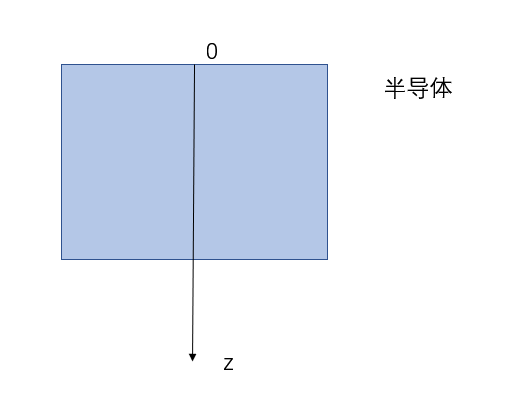
Subscriber老师您好,当外加电压之后,半导体内部会产生一个累积层,我想要计算并绘制出累积层内部载流子浓度与半导体顶部的距离的图像,请问这个如何进行操作呢?
-
February 24, 2023 at 9:27 pm
-
February 25, 2023 at 2:48 am
-
-
February 27, 2023 at 5:41 pm
Guilin Sun
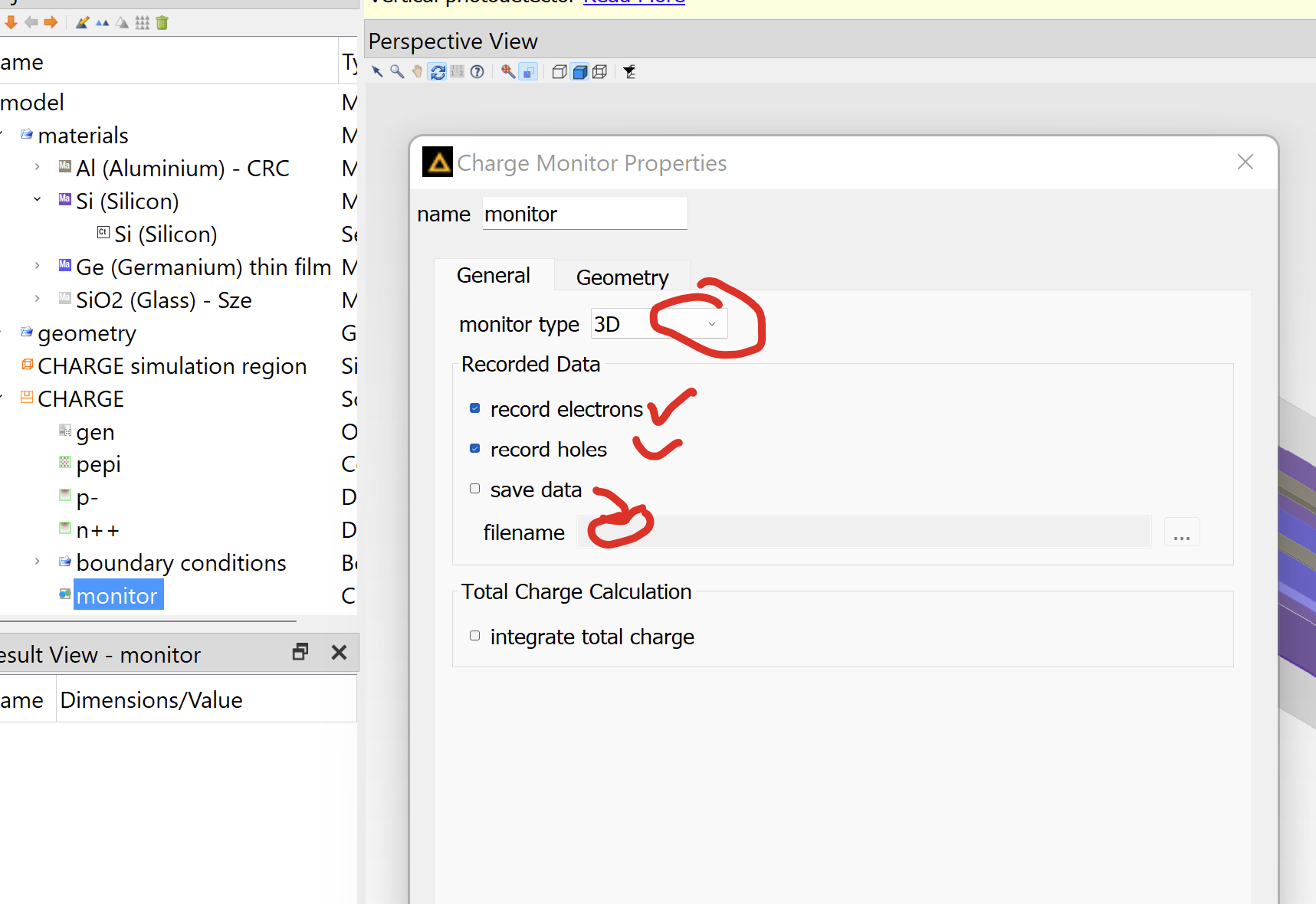
Ansys Employee你可以添加一个平面的CHARGE监视器。如果想用脚本,参见 addchargemonitor
网上脚本有点问题,因为是垂直与Y坐标轴,应该是
addchargemonitor;
set("name","charge");
set("monitor type",6); # 2D y-normal
set("x",0);
set("x span",5e-6);
set("y",0);
set("z span",5e-6);
set("z",0);
set("save data",1);
filename = "charge_data.mat";
set("filename",filename);
-
Viewing 2 reply threads
- The topic ‘计算半导体内部的载流子浓度’ is closed to new replies.
Innovation Space


Trending discussions


Top Contributors


-
5639
-
1885
-
1403
-
1303
-
1021
Top Rated Tags


© 2026 Copyright ANSYS, Inc. All rights reserved.
Ansys does not support the usage of unauthorized Ansys software. Please visit www.ansys.com to obtain an official distribution.


