-
-
November 29, 2022 at 1:49 am
Jiahui Huang
SubscriberDear Lumerical community,
I'm trying to simulate the band structure of a photonic crystal but having a problem decribled below:
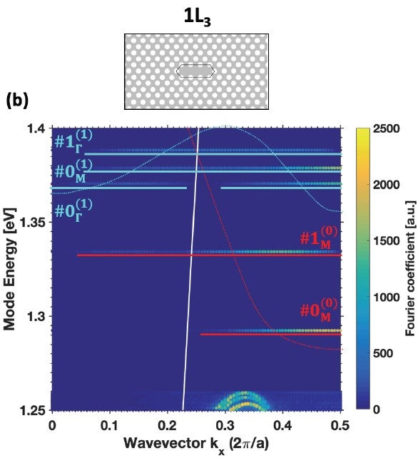
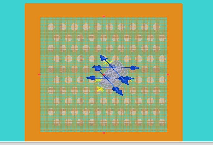
My goal is to simulate the band structure of a L3 cavity and it is expected to have localized energy dispersions as a function of k. To simulate band structure of a photonic crystal, Bloch boundry condition is a easy way. But for L3 cavity, I think if I use Bloch, I need to set the FDTD area to be sufficiently large.
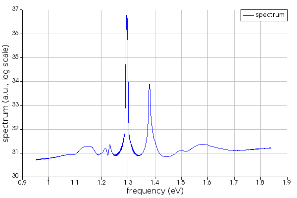
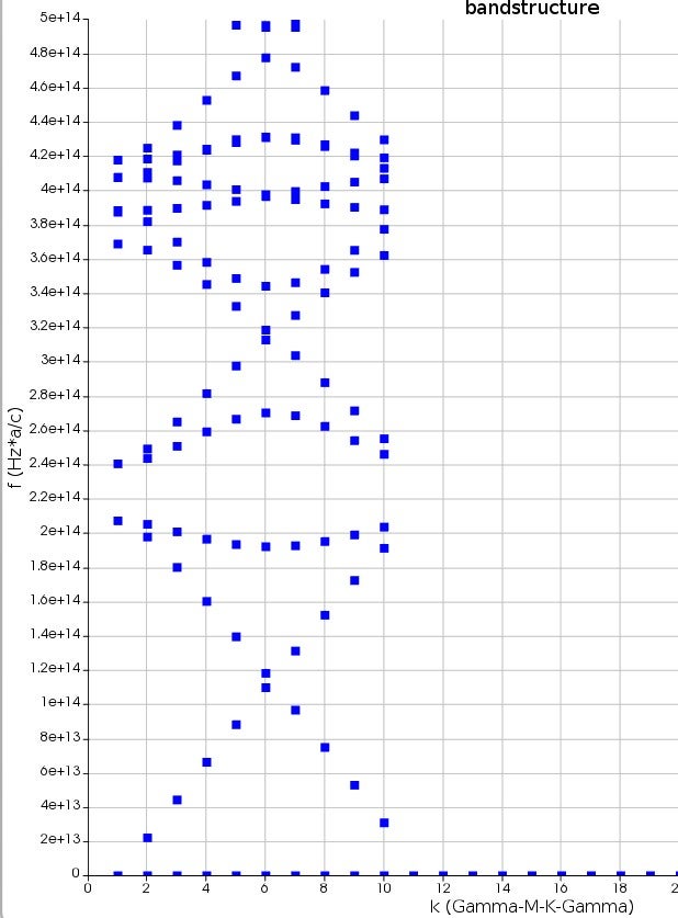
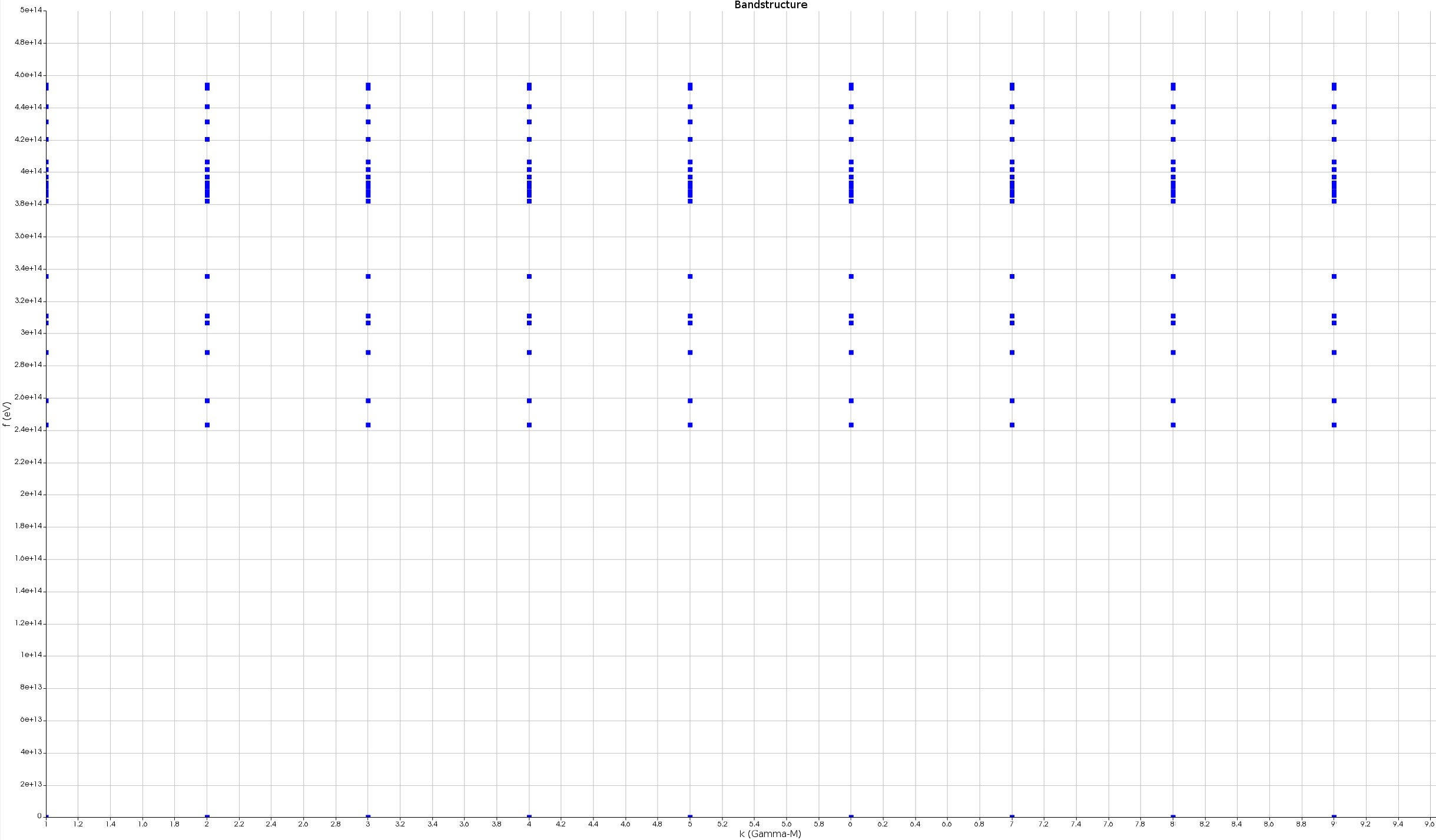
To begin with, I try to simulate the band structure of a photonic crystal (without cavity) with Bloch boundry condition and set FDTD area to be one unit cell of the lattice. I use this example: https://optics.ansys.com/hc/en-us/articles/360041567454. The result is below (I only plot the Gamma-M direction):
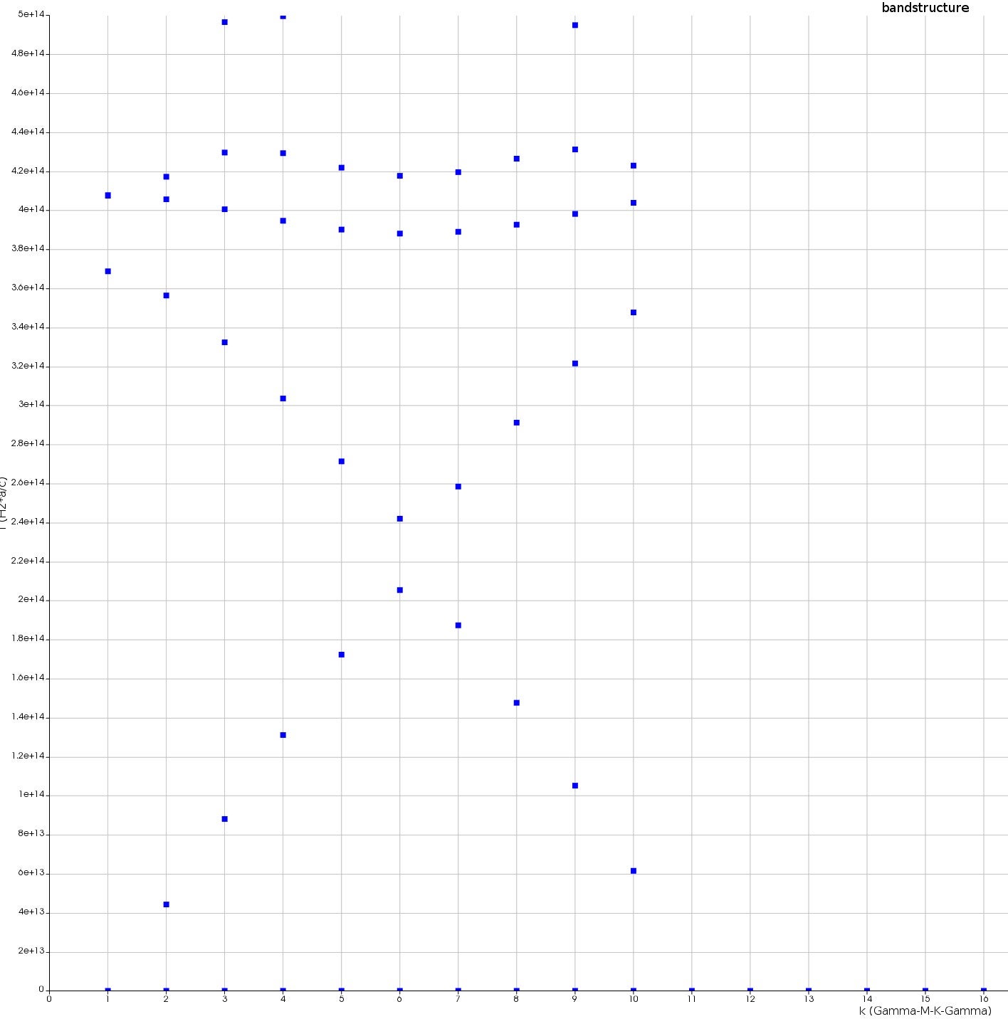
Then I want to increase the FDTD area to, e.g. 4 unit cells, to see whether I can reproduce the results. But I failed to do so as shown below:
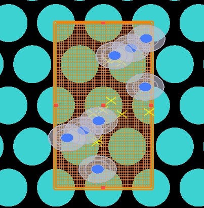
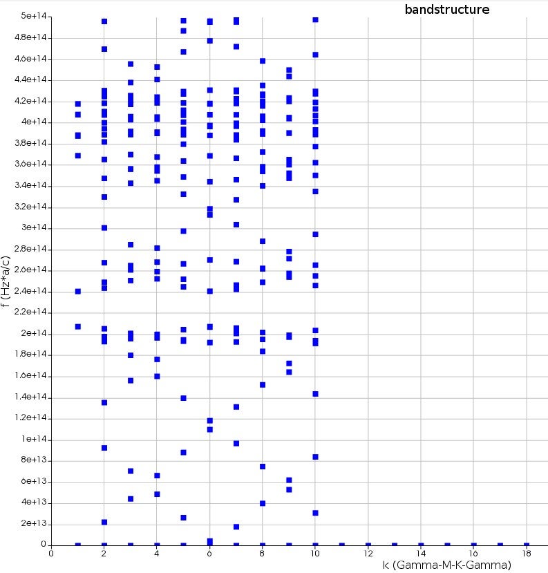
The right three results are generated when I played with the settings in "edit object" of the dipole cloud. But none of them reproduce the result by single unit cell simulation.
Â
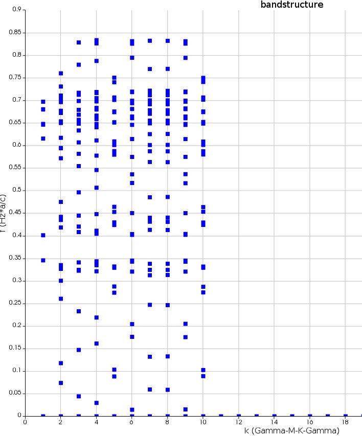
I also tried PML boundry condition with larger FDTD area. I can reproduce the bandgap but cannot reproduce the energy dispersion (it simply shows constant value).
I would appreciate if you have some suggestions. I can provide more information of my simulation if needed.
Â
Thank you!
Â
Â
-
November 29, 2022 at 9:19 pm
Guilin Sun
Ansys Employee1st, you should not increase the number of unit cells. Since it is peridoic, you will need to offset the phases of the dipole sources doing so. Please refer the example for hexagonal PhC exmaples.
Second, you cannot use PML without Bloch BCs. The findamental principle is to use the periodicity to find the band structure. Without it you will not be able to get the regular bands.
I am not aware of L3 band structure. Please find some related papers on this subject. Usually it is done from the band structure without defects. However, you can find resonance and stop bands for cavity. Please refer this exmple https://optics.ansys.com/hc/en-us/articles/360041567754-Photonic-crystal-cavity
Â
Â
-
November 30, 2022 at 1:17 am
Jiahui Huang
SubscriberHi Guilin,
Thank you very much for the reply. That makes sense to me. For L3 cavity and thanks to the example you mentioned, I'm able to plot the resonance:
But what I want to simulate is something show here where you can see localized modes marked by red and cyan horizontal lines:
It is from a thesis but the author only mentions he uses 2D FDM simulation. Do you have any comments on this? Thank you!
-
-
November 30, 2022 at 7:52 pm
Guilin Sun
Ansys EmployeeI thought I replied but it seems it failed.
You may need to refer the reference for more details.
I guess that, the vertical axis is equivalent to frequency, and the horizontal axis is equivalent to effective refractive index of the modes. If you can somehow get the effective index, you can get the actual propagation constant beta=k0*neff, where k0 is the wavenumber in vacuum. then you can tranform it to the Block wave vector.
Â
To get the mode effective index, you can use the formula from Sneider and Love's book, which gives the expression of neff as a function of the mode fields.
Or you can use FDE to find the neff for this 2D cross section cavity as an infinitely long waveguide.Â
Those are what I can think of and suggest , since there is no exmaple on Lumerical website.
-
August 20, 2023 at 4:56 am
Muhammad Danial Haziq Azizan
Subscriberhye, how do you get 4 graph bandgap structure? I try to run the script but only obtain 1 result for the TM mode
-
August 21, 2023 at 3:52 pm
Guilin Sun
Ansys EmployeePlease refer to the example Bandstructure of planar photonic crystal with a hexagonal lattice
-
- The topic ‘band structure simulation problems’ is closed to new replies.
-
5849
-
1906
-
1420
-
1305
-
1021
© 2026 Copyright ANSYS, Inc. All rights reserved.


