-
-
September 18, 2021 at 4:29 am
ha_nguyen3
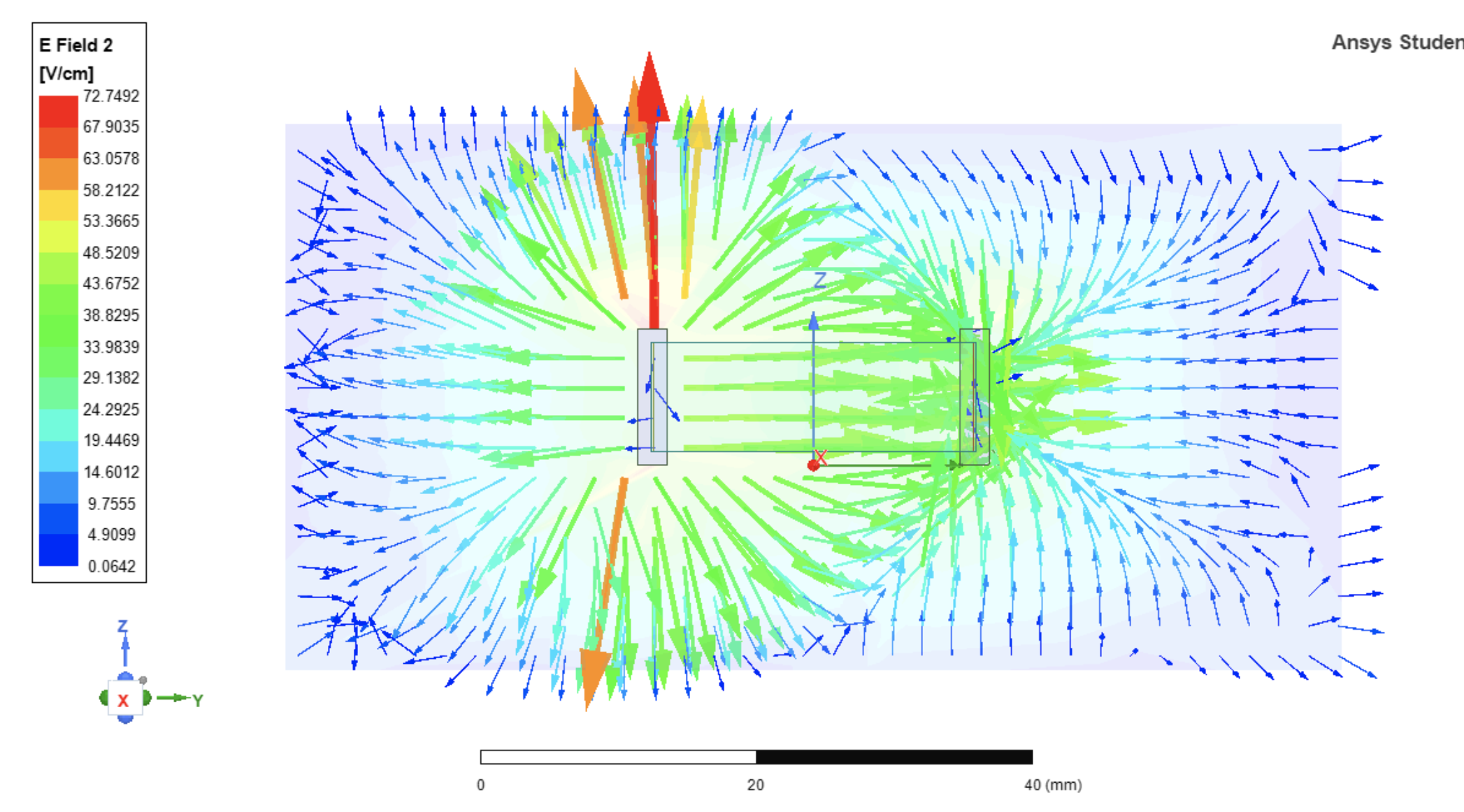
SubscriberI used lumped port to assign excitation. The blue sheet is a port. The yellow plate is a copper embedded in an insulating material with e of 5000. The purple plate is assigned to GND, and also embedded in the same insulating material.
The field vector is what I expect how the field would behave. Most fields should go straight through the insulating layer to get to the other side. I also expect that the E-field should be strongest in the insulating layer that cover around the metal plate, but the map shows that isn't a case. The air had the strongest field , and almost no fields exhibit in the insulating layers or layers between 2 plates.
I don't know why and what I have done wrong.
Note: I want to study electric field across the model at 42V and 200kHz (electrodynamics). My boundary medium is air. I'm using HFSS in Ansys Electronics Desktop - Student version.
Thank you.
September 20, 2021 at 7:24 amAncS
Ansys Employee
Since there is an inverse relationship between the E field and relative permittivity of the material, the field inside the insulator cover is 5000 times less than that of in air (As you mentioned that the relative permittivity of the insulator material covering the metal plates is 5000). That's why the plot shows the negligible magnitude of the E field inside the insulator having high relative permittivity. Air has the least relative permittivity so the E field is highest there.
Hope this clears your doubt.
All the best!
Regards
Anchal
September 20, 2021 at 5:08 pmSubscriber
I believe that would be a case if only one side of the metal plate is covered by an insulator. In this case, rather than going through the insulator, the fields would go around the insulator to reach the other plate.
In my scenario, the metal plate is completely embedded in the insulator. My hypothesis is that since the metal plate is covered in all four sides, the fields are forced to go straight through the insulator even if the insulator has a dielectric constant of 5,000. It is because the fields would choose the shortest route to reach the other plate. As a result, most fields should concentrate in the insulator and drop at the air gap. With this in mind, the field strength is expected to be highest in the insulator.
Please let me know your thoughts.
Thanks Ha Nguyen
September 20, 2021 at 5:14 pmPraneeth
Ansys Employee
May I know why you were using dielectric constant of 5000? I think it is very huge value.
To make sure that the setup is correct can you run a more simpler case removing the insulator.
Please run a simple parallel plate capacitor model and validate the design by observing the results.
You can also check dielectric filled parallel plate capacitor model.
All the very best.
September 20, 2021 at 5:54 pmSubscriber
I use e of 5000 for the insulator because in theory, high dielectric material helps to improve the capacitance of the electrodes (the metal plate), thus reducing the electrodes' impedance to the applied AC signals. This helps to reduce the voltage drop in the electrodes, so that larger applied voltage appears across the tissues (aka other layers between two insulators/plates). The ultimate goal is to achieve the E-field between 1-3V/cm in circle solid in the geometry.
In short, e>5000 is the recommended constant for my study regarding tumor treating fields.
Here are my control setup.
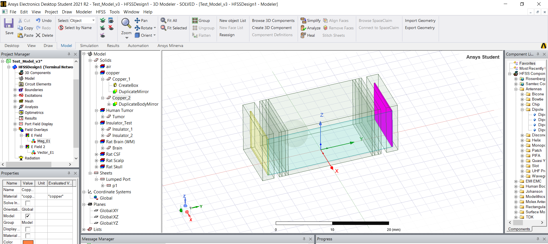
In case 1, I only have copper plates. As expected, the fields are going in all directions.
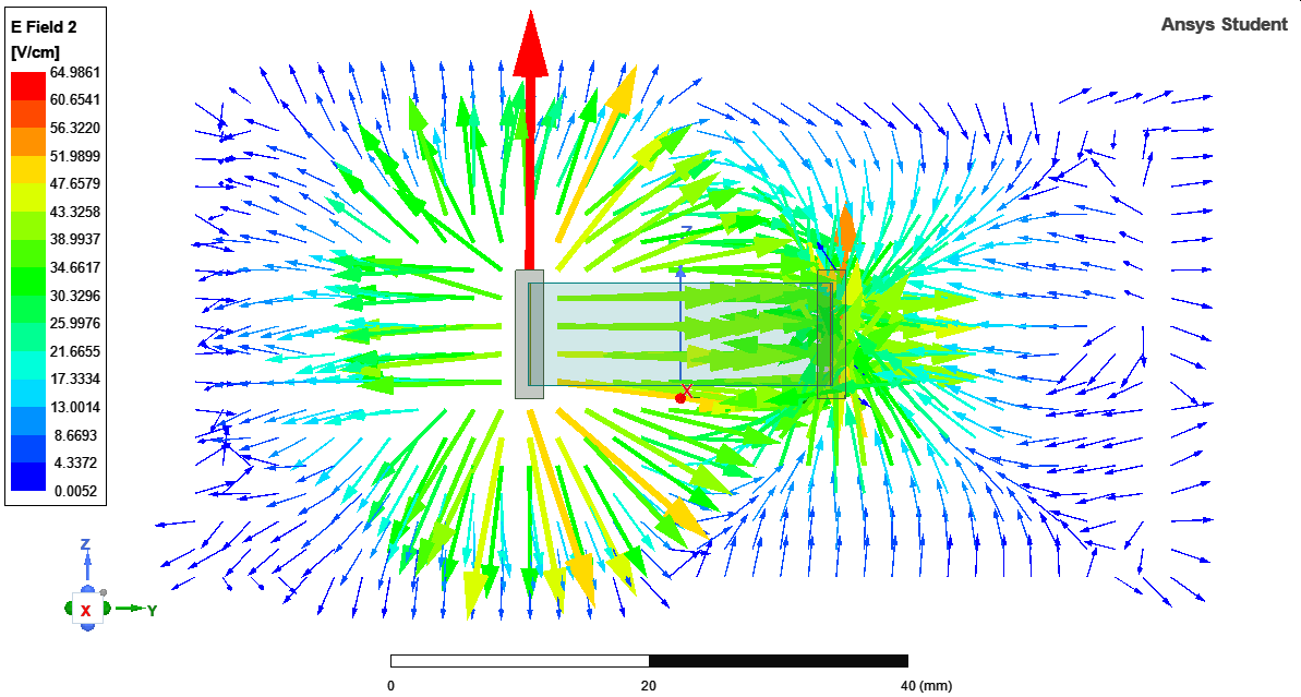
In case 2, three sides of the coppers are covered by an insulator, leaving one end exposed to the air - this is where the port is connected to. I'm little confused why most fields go vertically, rather than going horizontally through the insulator. Again, almost no fields in the insulator...
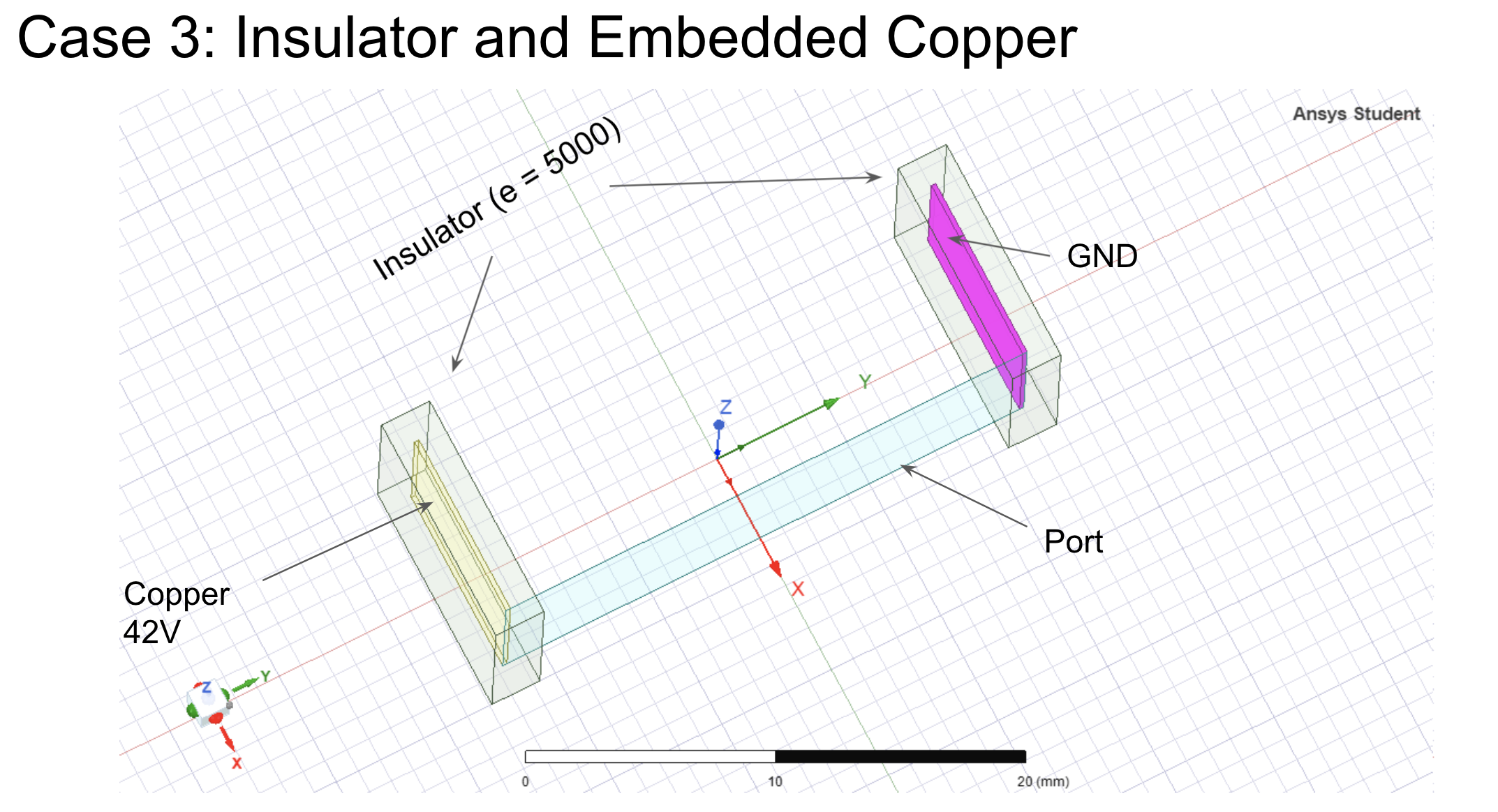
The purpose of case 3 is to study how the port's placement affects the fields. In case 3, all four sides of the copper plates are covered by an insulator. The port has to cut through the insulator. The fields drastically drops, compared to that in case 1 and 2. So I assume the port's placement has an impact on the simulation results, but I'm still confused why this happens.
Does the results of control setup look appropriate to you?


 Sorry for a length post. Thank you.
Ha Nguyen
September 20, 2021 at 5:58 pmSubscriberAnd how can I access the dielectric filled parallel plate capacitor model?
Thanks Ha Nguyen
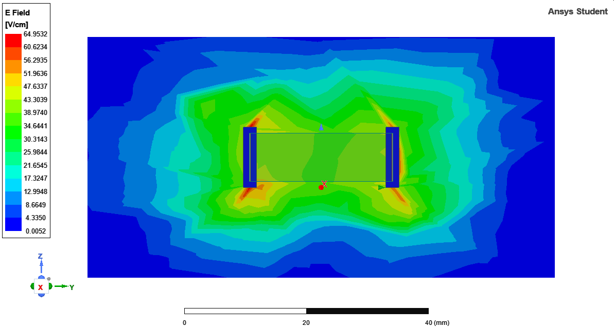
September 21, 2021 at 12:19 amSubscriberOops, I found a mistake in Case 3. I put 1V instead of 42V. Sorry for the confusion.
These are the correct results of Case 3 - Embedded Copper. Regardless, this case still provides the lowest E-field, and most fields concentrate in the z-direction. So I guess it is safe to say the port placement does affect the simulation.
Viewing 6 reply threads- The topic ‘E-Field in insulator’ is closed to new replies.
Innovation Space Trending discussions
 Top Contributors
-
peteroznewman
 6680
6680 -
scabo
 1906
1906 -
Dennis Chen
 1469
1469 -
javat33489
 1313
1313 -
Shyam Prasad V Atri
1022
Top Rated Tags
© 2026 Copyright ANSYS, Inc. All rights reserved.
Ansys does not support the usage of unauthorized Ansys software. Please visit www.ansys.com to obtain an official distribution.
-
Ansys Assistant will be unavailable on the Learning Forum starting January 30. An upgraded version is coming soon. We apologize for any inconvenience and appreciate your patience. Stay tuned for updates.