Photonics

Photonics

Topics related to Lumerical and more.

FDTD and Bandstructure size and mesh size

    • Infinite
      Subscriber

      Hello, For bandstructure and dispersion calculation, should FDTD region has to be the same side of a period size?

      what is the condition for 1D and 2D bandstructure calculation and FDTD size? Also for 1D say only for ky dispersion curve can I put block BC for both y and x direction, provided the dipole source is z direction.

      I noticed a lot of simulation when I increase the FDTD region size to the period size of the periodic structure then all the bands fall in a line (in same frequency for all ky values). but same set up if I lower the FDTD size to much smaller size compared to the period size then I can see those bands. Please let me know how to resolve this?

      Thank you

    • Infinite
      Subscriber
      Hello, can anyone help?
    • Infinite
      Subscriber
      Hello Ansys Employees, Anyone please answer this question, It has been so long.
      Thank you
    • Guilin Sun
      Ansys Employee
      Hi, There! Sorry to reply you late.
      "For bandstructure and dispersion calculation, should FDTD region has to be the same side of a period size?"
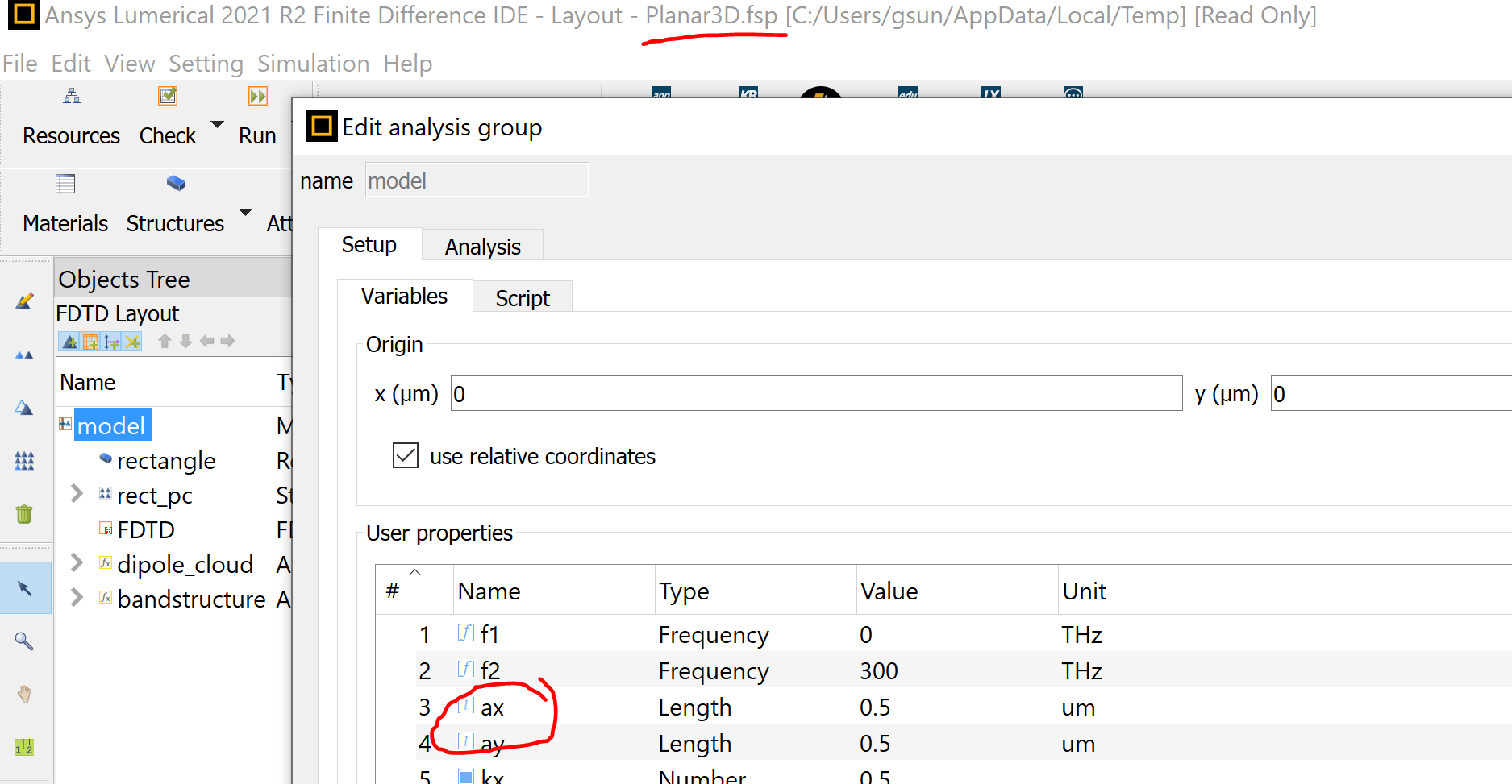
      As a rule of thumb, FDTD region should match the periodic boundary when it is periodic, eg, infinitely periodic. The simulation span determines what is the period. However, since the structure is periodic, it has no beginning or ending point. so you can set the location of the periodic boundary any where as long as the simulation span is one period. My suggestion is to position the periodic BCs at relatively uniform area.
      "what is the condition for 1D and 2D bandstructure calculation and FDTD size? "
      As mentioned before, in the periodic axis, the FDTD size or span must be a period, whether it is 1D or 2D
      "Also for 1D say only for ky dispersion curve can I put block BC for both y and x direction, provided the dipole source is z direction."
      Bloch BC is a periodic BC and can only be used in periodic axis. In your case, Y axis is periodic, but x axis is not. so x and z axis should use PML BCs.
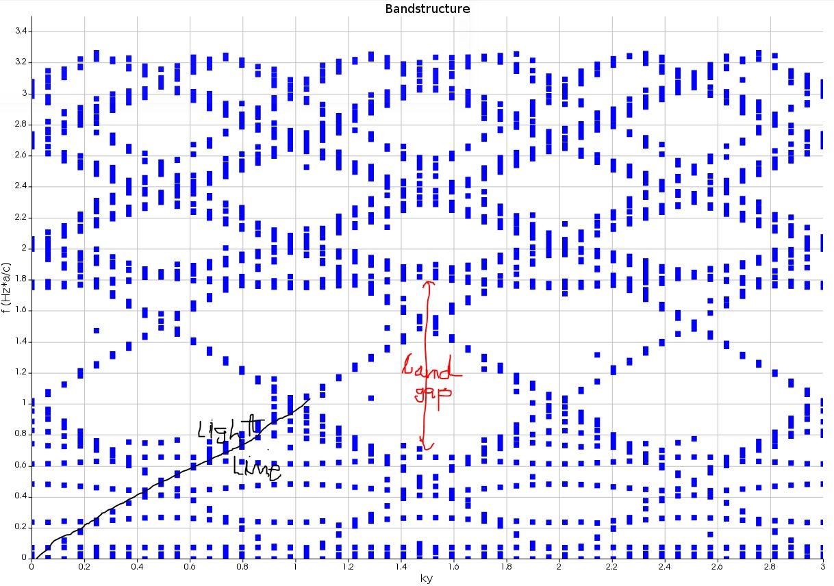
      "I noticed a lot of simulation when I increase the FDTD region size to the period size of the periodic structure then all the bands fall in a line (in same frequency for all ky values). but same set up if I lower the FDTD size to much smaller size compared to the period size then I can see those bands. Please let me know how to resolve this?"
      You should not change the FDTD size or spans other than ONE period in periodic axis. Please refer the online examples:
      https://support.lumerical.com/hc/en-us/sections/360006919074-Photonic-crystals
    • Infinite
      Subscriber
      Thank you Mr. gsun.
      My structure is periodic both x and y with different period size, but I was trying to calculate only one direction Ky.
      If I use PML to y in this case then the simulation does not converge, I mean with time the auto-shout off values keep increasing and no value recorded from the sweep.
      Then I increase FDTD a lot in x- direction (much more than the period), but still the simulation auto-shutoff keep increasing.
      Only if I made y-direction FDTD much smaller and x-block then I can see some bands.
      but I know that is not recommended, to reduce FDTD size smaller than period, So what is meant by a totally flat band structure?
      I can not even see the light lines even no matter how many band I choose to view. or how much ky, and frequency range I increase.
      I have a 800 nm periodicity y and and 350 nm period in x direction and, with metal nanomaterial of 40 nm thick over 40 nm thick dielectric, and dielectric is over 110 nm thick metal. In this case if I want to calculate bandstructure and dispersion for ky then what should be the FDTD size in x and z direction please?
      In the model should I manually insert the information of the lattice type, say Rectangular lattice? How can I do that please?
      Thank you
    • Guilin Sun
      Ansys Employee
      If both xy are periodic, you will need to use Bloch BCs in both axes, and will also need to specify kx, and I guess you want kx=0;
      As replied early, you will need to set x spa and y spa to be the px and py which are the periods in xy.
      As for the lattice, if it is rectangular you should use it.
      You may need to learn something more about periodic structures and their properties, which is fundamental doing such simulation.
      As for no bands or light lines, you will need to adjust simulation time, in order to capture the proper part of signals. If the simulation is too long, only frequencies with high Q are left. Please refer some examples and check their settings.

    • Infinite
      Subscriber
      Thank you Mr. gsun.
      The only question remains, how can I add this information to the model so simulation will know what type of lattice it is?
      Thank you
    • Guilin Sun
      Ansys Employee
      I do not know how did you create your simulation file. If it is from the example, it is lattice dependent. Once you choose rectangle lattice, you can modify to have ax and ay differently. In this example:
      Bandstructure of planar photonic crystal with a square lattice you can see it has ax and ay. what you need is to assign them different values.

      You can also write your own script in the model to meet your specific requirements.
    • Infinite
      Subscriber
      Thank you Mr. gsun.
      Following all the information you have provided, this is what I got in attached pic.
      So please let me know is the light line and band gap seems to correct.
      The question for the metal and dielectric layer structure with periodicity, how can I obtain the dispersion curve from here please?
      Thank you for a lot of help.
    • Guilin Sun
      Ansys Employee
      For 3D band structure simulations, if the geometry has symmetry, please use symmetry BC to separate TE and TM modes; if there is no symmetry, please set the dipole polarization properly to isolate them. otherwise the bandstrucures are mixed, it can be difficult to extract information correctly.
      The light line seems ok but the bandgap seems there but difficult to quantify.
      In addition, it seems you simulated more than one period or Ky larger than irreducible Brillouin zone ? please make sure the simulation settings fulfill the requirements.
      Once you have correct band structure, you should be able to convert it to dispersion curve, since you have frequency and K values. You may need to find some reference on this.

    • Infinite
      Subscriber
      Hello Mr. gsun
      Thank you very much for quick response.
      I already set polarization on dipole source, so these all results are for one particular polarization as well as the previous pic I sent.
      I am simulating only one periodic cell, and this simulation is bound to be for one periodic cell as default set by ax and ay.
      My structure is periodic on both x and y, and symmetric with respect to x but not with respect to y.
      So when I am calculating bandstructure for ky, I should use symmetric BC for both x_nim and x_max right?
      Please see the fig a2 when I am using symmetric BC for x_min and PML for x_max. and it just a flat fine with all same condition.?
      I am calculating only Gamma-Y, So do you think I need to add X-M sweep also for Kx to getting ky correctly as it is 3D simulation?
      Also how to calculate the ky value for irreducible Brillouin zone except pi/ay? Please see the fig a1 when I changed ky with this condition.
      Thank you
Viewing 10 reply threads
  • The topic ‘FDTD and Bandstructure size and mesh size’ is closed to new replies.