-
-
July 1, 2021 at 3:50 pm
Prateeksha
SubscriberHi,
I am trying to design grating tunable reflector based on thermal simulation. I have few queries related to it, such as;
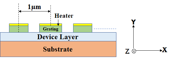
1) Is it meaningful to simulate unit cell in thermal solver and use the same thermal profile in optical solver for periodic structure? For example, my unit cell period is 1 um, but I can not keep my thermal simulator boundaries restricted to unit cell dimensions. It should be large enough for converging the results. I observed that if I keep smaller simulation domain (eg. 1 um) and then increase it gradually, results keep changing and it gets saturated after certain lateral dimension. Basically simulation domain should be kept large enough and for that I need to expand lateral dimensions (x-axis) of substrate and device layers also, which is not the same as unit cell dimensions (1 um). In that case, grating is the replica of optical simulation, but substrate and device layer won't be the same. Heater is placed on the top of the grating, so this heat won't be restricted to 1 um unit cell, infact it will flow through the complete device layer.
2) Since, it's a periodic structure, so heat source will also be repeated, so won't there be any cross heating effect? How to include this effect into simulation?
July 3, 2021 at 2:11 amKyle
Ansys Employee
Is the heat only applied to one of the gratings, or all of them? If it is applied to all of them then the simulating is periodic and you can use insulating BCs in the HEAT simulation to represent periodic boundary conditions. Insulating BCs represent periodic boundaries because the temperature is expected to be the same at either side of the interface between the unit cells, so there will be no heat transferred between the unit cells.
July 3, 2021 at 6:49 pmSubscriberHi Yes, heat is applied to all the unit cells, so basically heat source is also periodic. As you mentioned, insulating boundary condition won't allow heat to flow from one unit cell to other. But it won't be the same case in real device. There might be heat flow from one unit to other since periodicity of device is just 1 um and heat source is 0.8 um in x-span. I want to include cross coupling effect also.
Thanks
Prateeksha
July 4, 2021 at 8:08 amSubscriberHi I have few more questions regarding your replies. such as;
1) In that case only unit cell needs to be simulated not the complete structure with so many periods, is it?
2) Can we restrict simulation domain also till 1 um i.e. equal to period of device? There is no need to make simulation domain very large, is it?
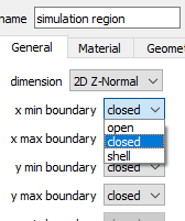
3) Insulating boundary condition can be applied at xmin and xmax (in the direction of periodicity) of simulation domain, is it?
4) Will these settings give temperature profile of unit cell or a periodic structure? Because further temperature profile needs to be used in optical simulation also.
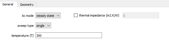
5) What about following settings:
 Looking forward to your reply!!
Thanks
Prateeksha
July 6, 2021 at 4:12 pmSubscriberHi Kindly reply to my previous queries.
Thanks
Prateeksha
July 6, 2021 at 11:20 pmAnsys Employee
Sorry for the delay. You're correct that the insulating boundaries will not allow heat to transfer between the unit cells. However, because the temperature will be the same at each edge of the unit cell there will be no heat transfer between the cells in the device either. So the insulating boundaries properly model the periodic boundary conditions in this case.
1) In that case only unit cell needs to be simulated not the complete structure with so many periods, is it?
Yes, for a periodic structure only one cell should have to be simulated for both the thermal and optical simulations.
2) Can we restrict simulation domain also till 1 um i.e. equal to period of device? There is no need to make simulation domain very large, is it?
For a periodic simulation the simulation domain should generally only contain one unit cell in the periodic direction, there is no need to make the simulation region larger.
3) Insulating boundary condition can be applied at xmin and xmax (in the direction of periodicity) of simulation domain, is it?
Yes, that's correct. The other boundaries will most likely use other boundary conditions, similar to this example:
4) Will these settings give temperature profile of unit cell or a periodic structure? Because further temperature profile needs to be used in optical simulation also.
The monitor data will be only a single unit cell. However, this should be enough for the optical simulation, because the optical simulation will only contain one unit cell. If need be, the HEAT monitor data could also be duplicated to make the thermal profile for multiple cells.
5) What about following settings:
These should all be closed in this case, because we want the simulation boundaries to be the boundaries of the "HEAT simulation region" object.
Please let me know if you have any questions.
July 7, 2021 at 10:28 amSubscriberHi Thanks for your reply!!
I have few more queries, such as;
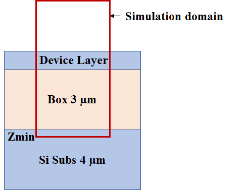
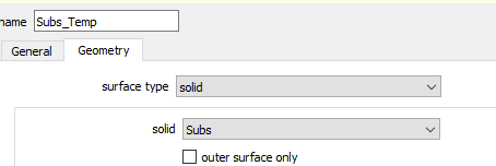
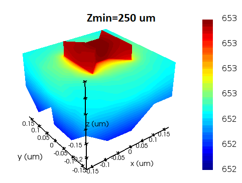
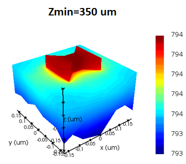
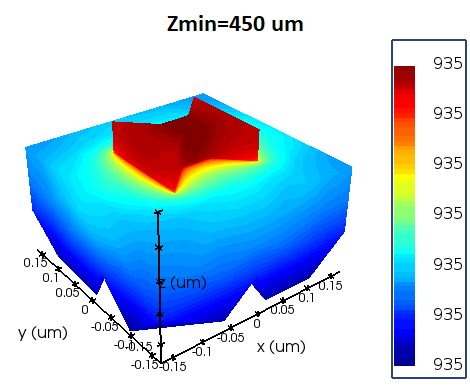
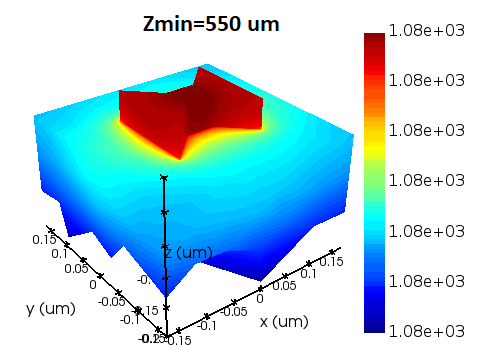
1) In the following example https://support.lumerical.com/hc/en-us/articles/360041686234, Z span is taken very large more than 250 um and Zmin is kept at 300 k. Is there any specific reason for using such a thick substrate? In my structure, device layer is placed on 4 um Si substrate and 3 um silica box layer, which is same as optical simulation. Can I use 300 k temperature boundary condition for Si substrate or I need to take very thick substrate and keep Zmin at 300 k? In both the cases results will be different. Please see the attached figures for reference.
 2) My working wavelength is 1550 nm and I have chosen my material properties from https://refractiveindex.info/?shelf=main&book=HfO2&page=Al-Kuhaili, Material Properties of HFO2 is not available in optical solver, but it's available in Heat solver. Refractive index of HFO2 is 1.8777 and from eps=n^2, its dielectric permittivity should be 3.525 but it is given as "25" under electronics properties. It's the same case for silica also, these not obeying the square relationship. Does Heat solver use these values of relative permittivity for some different wavelength? What about the thermal properties? Are these independent to wavelength, as we don't have any option to fix the operating wavelength?
Looking forward to your reply!!
Thanks
Prateeksha
July 8, 2021 at 1:44 amAnsys Employee
1) I don't think it would be accurate to fix the temperature at room temperature a few microns from the heater, I think this would only be valid for a thick substrate. I would recommend that you extend the simulation region a large distance into whatever is below the Si layer, similar to the example.
2) These dielectric properties are for the electrical solver CHARGE. They are the DC permittivities, which is why they're different than the permittivity at optical wavelengths. The HEAT solver doesn't use these electrical properties, it only uses the thermal properties. The HEAT solver is only solving the heat equation, so the wavelength of the light isn't relevant for this simulation. The HEAT solver is used first to calculate the temperature distribution, which is then imported to an optical solver like FDTD or DGTD for the optical simulation.
July 11, 2021 at 11:18 amSubscriberHi
Thanks for your reply!!
I have few more queries, as;
1) How long the simulation region should be extended into the substrate? I performed few tests and found that temperature profile is continuously changing with simulation domain (into substrate) and temperature is increasing on increasing the simulation domain. The available example also shows the same behavior. In optical simulation, I just used 3 um of box and 4 um of silicon (total 7 um), below the Si device layer. In real device, bulk Si might be around 500 um thick, but what's the optimum heat simulation distance in substrate, since results are not converging? Is substrate thickness important for optical domain also?
2) In the given example, they have used imported heat source, but in my case I am using 1nm of Graphene layer as a Heater. Since the Graphene is not available in heat solver library, so I defined like https://support.lumerical.com/hc/en-us/articles/360042273534-Transient-heat-flow-in-a-graphene-coated-glass, but here they used very thick layer of Graphene. My concern is, Can I used a thin layer (1 nm) of Graphene as a Heater? I have applied Uniform Heat source to it and found that even after changing the material properties of thin Heater (instead of Graphene some other material), results are not changing. It's not dependent on the material properties of the Heater, is it ok? Even on increasing the thickness of Graphene Heater to 20 nm, then also temperature profile is same in the device layer. What might be the possible reason?
Looking forward to your reply!!
Thanks
Prateeksha
July 11, 2021 at 12:19 pmSubscriberHi I want to add one more thing, thermal conductivity of SiO2 is 1.38 W/mK, which is much smaller than Silicon's conductivity i.e. 148 W/mK. So basically SiO2 is good heat insulator which is placed in between the device layer and bulk Si, then also temperature in the device layer is highly dependent on simulation domain in bulk Si substrate, why so?
Thanks
Prateeksha
July 13, 2021 at 8:24 amSubscriberHi Kindly reply to my queries!!
Thanks
Prateeksha
July 15, 2021 at 2:36 amAnsys Employee1) A large distance might be required, as in the Photothermal heating in plasmonic nanostructures example. The exact distance required should be determined by convergence testing, where you increase the distance until the results converge. This distance doesn't need to be as large in the optical simulation, as absorbing boundary conditions can be used in DGTD.
2) Monolayer graphene is a 1D material so it is difficult to model in HEAT, but a very thin 3D object would be the best way to model. If you're using a uniform heat source over a very thin layer I think it's reasonable that the material properties of the layer wouldn't affect the simulation results very much, as the heat source is applied to the entire object and there isn't very far for the heat to travel through the layer.
3) The SiO2 would offer some insulation between the device layer and bulk Si, but it might not be entirely isolating the bulk Si from the heater, so the location of the boundary in the bulk Si might still affect the results in the device layer.
July 15, 2021 at 12:46 pmSubscriberHi Thanks for your reply!!
I have few more queries:
1) I have tried increasing substrate thickness and simulation span in Z-direction in the Photothermal heating in plasmonic nanostructures example, but I didn't get any convergence. This I tried with both that is diabolo and dipole examples. I am getting convergence in my simulations also. Why is the temperature increasing on increasing Z min?
 2) This example also uses heater at only few micrometers from boundaries, but I checked here increasing the Ymin https://support.lumerical.com/hc/en-us/articles/360042833673-Thermally-tuned-waveguide-FDE-and I get convergence of results at small distances. Is the bigger simulation region related to periodic structure only?
Thanks
Prateeksha
July 20, 2021 at 8:31 amSubscriberHi Kindly reply to my queries!!
Thanks
Prateeksha
July 22, 2021 at 3:21 pmSubscriberHi I am waiting for your reply!!
Thanks
Prateeksha
July 23, 2021 at 10:14 pmAnsys Employee
Sorry for the delay in replying, I'm not sure of the answer to your questions so I am discussing this with a colleague with more experience in this type of simulation. I will let you know when I have more information.
July 24, 2021 at 5:43 pmSubscriberThank you for your reply!!
Kindly discuss and let me know soon.
Thanks
Prateeksha
July 27, 2021 at 3:55 amAnsys Employee
1) Sorry again for the delay. My colleague has told me that I was mistaken earlier, we don't expect to see the results converge to a single solution when moving the fixed temperature boundary condition away from the device. In the example, it is assumed that the bottom of the substrate is fixed at room temperature and the entire thickness of the substrate is included in the simulation. The thickness of the substrate is an important parameter in this example, and has a significant impact on the results. If you'd like to take the same approach as the example, the entire thickness of the substrate should be included in the simulation region.
2) This example actually uses the same boundary conditions as the photothermal example, but from the temperature map results it looks like most of the heat is lost to convection in the air above the SiO2, so the x and y min boundary conditions have less of an impact on the results.
July 29, 2021 at 8:00 amSubscriberThank you for your reply!!
Viewing 18 reply threads- The topic ‘Heat Solver Simulation for periodic structure’ is closed to new replies.
Innovation Space Trending discussions
 Top Contributors
-
peteroznewman
 6765
6765 -
scabo
 1906
1906 -
Dennis Chen
 1490
1490 -
javat33489
 1330
1330 -
NickFL
1127
Top Rated Tags
© 2026 Copyright ANSYS, Inc. All rights reserved.
Ansys does not support the usage of unauthorized Ansys software. Please visit www.ansys.com to obtain an official distribution.
-
Ansys Assistant will be unavailable on the Learning Forum starting January 30. An upgraded version is coming soon. We apologize for any inconvenience and appreciate your patience. Stay tuned for updates.