TAGGED: mechanical, pcb-manfacturing, shell-elements, spaceclaim, thermal-stress
-
-
June 28, 2021 at 5:19 am
warrensu
SubscriberMy analysis needs to focus on the layer level (~10^-6) scale, for example, how a layer of copper, dielectric, or solder mask contributes to the overall bending (thermal strain) of the board in a reflow oven.
Since a PCB model usually contains very intricated designs, modelling each layer of the PCB as 3D solids is going to be computationally expensive and will result in huge mesh element count. The approach I have in mind is modelling each layer as a 2D surface (or shell? Not really sure how the two are different) in Spaceclaim first, then in Mechanical specify the geometry thickness. Would this allow me to simulate PCB warpage in the out of plane direction as well?
Please let me know if this approach is conceptually correct or could be improved in any way. Thank you very much.
Side note: I am aware that Ansys has a feature called trace mapping, however, I've been having troubles to import layer stackup information into Mechanical properly. So I am wondering if there is any other workaround for now.
June 28, 2021 at 4:57 pmRahul Kumbhar
Ansys EmployeeI don't see any issue with your approach. You should be able to get the out of plane warpage. You can try simple test to verify this.
June 29, 2021 at 9:23 amwarrensu
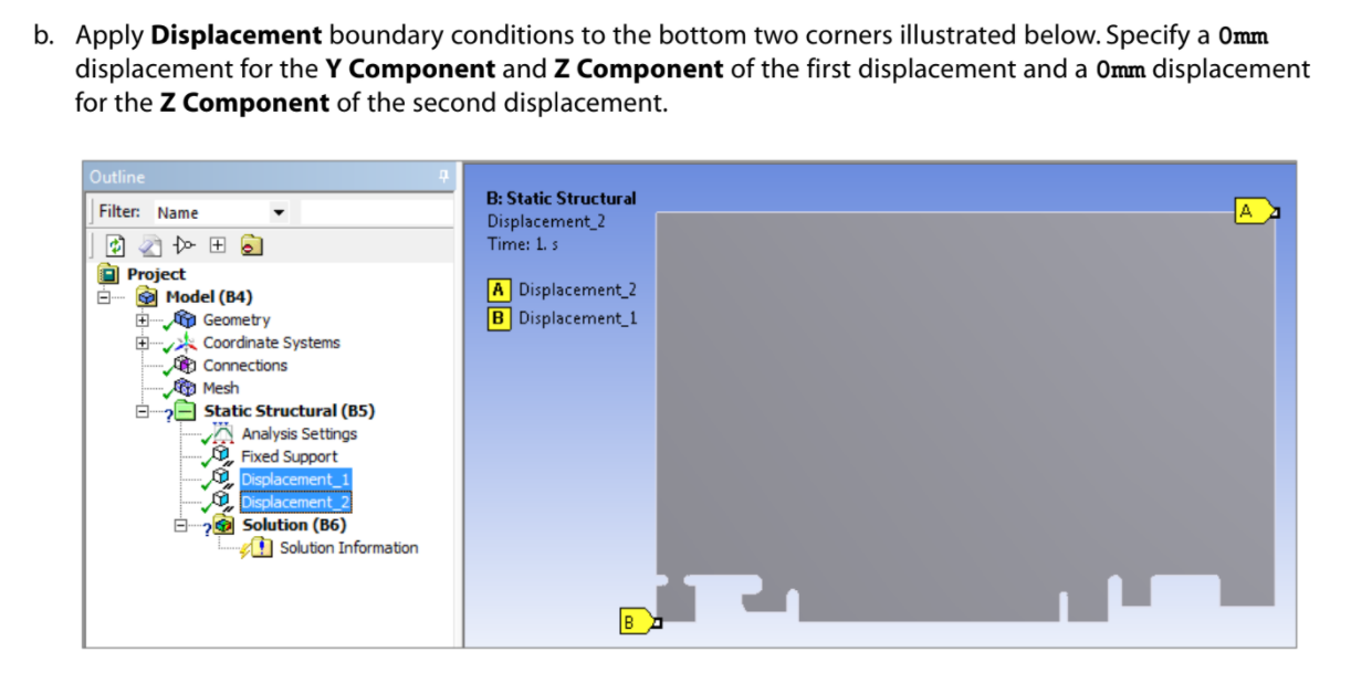
SubscriberThank you for the suggestion! The preliminary tests show reasonable results. Now I am hoping to figure out how would my boundary conditions affect the accuracy of my simulation. Currently, I have a thermal condition that heats the entire board from room temperature to 260 degrees Celcius (500 F), which is the maximum temperature in a reflow soldering oven. So far, I've attempted two setups: 1. Place a fixed support at the center node of the board 2. Place a fixed support at bottom right corner, a displacement [X: Free, Y: 0, Z: 0] at bottom left corner, and another displacement [X: Free, Y: Free, Z: 0] at top right corner (as shown in the image). This second approach is something I found in an Ansys presentation. One problem I found with the second approach is that I am interested in warpage out of plane, so a Z = 0 displacement condition would certainly affect my results. Whereas, the first approach would essentially be assuming that something is pinning down my board which doesn't exist in reality in a reflow oven. Please let me know if my thinking is correct, and also, any other boundary conditions that I could consider!
June 29, 2021 at 10:08 amRahul Kumbhar
Ansys EmployeeI think both process give somewhat similar deformation but opposite. I would suggest second method because it is not pinning down the centre. In second case max deformation will be at centre while in first case max deformation will be at corners.
June 30, 2021 at 5:53 amwarrensu
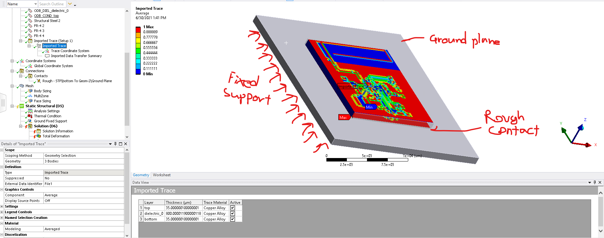
SubscriberI came up with a third boundary condition setup as follows:
Create a large plane geometry for the PCB to sit on
Place fixed support on the plane geometry (for the purpose of simulating the "ground" in a reflow oven)
Set a rough (or maybe frictionless?) contact between the ground plane and PCB (To allow a gap to form when the PCB bends)
However, this setup unfortunately did not converge when I tried running it. Any suggestion for improvement is appreciated!
June 30, 2021 at 5:58 amRahul Kumbhar
Ansys EmployeeSeems to be ill-condition issue. You can try turning on small sliding. Also use large number of substeps.
June 30, 2021 at 9:14 amwarrensu
Subscriberthanks for all the amazing suggestions. I figured out by placing a displacement [X: 0, Y: 0, Z: Free] on the bottom face matches the outcome I'm expecting.
Viewing 6 reply threads- The topic ‘Modelling PCB warpage in Ansys Spaceclaim and Mechanical’ is closed to new replies.
Innovation SpaceTrending discussionsTop Contributors-
5824
-
1906
-
1420
-
1305
-
1021
Top Rated Tags© 2026 Copyright ANSYS, Inc. All rights reserved.
Ansys does not support the usage of unauthorized Ansys software. Please visit www.ansys.com to obtain an official distribution.
-


