

-
-
May 12, 2021 at 4:08 pm
bsr
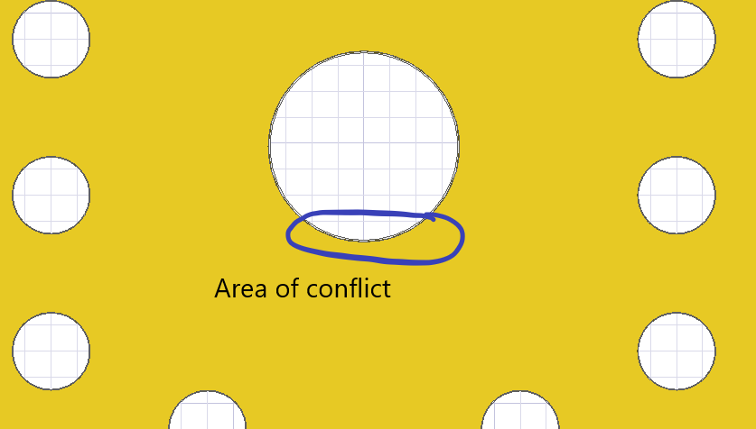
SubscriberThe exported design in Q3D displays an air gap in between a via and adjacent copper plane. Could you please suggest some options with which there are no such flaws in the geometry?
In the following figures I am displaying a flaw as well as all the options used for exporting the file to Q3D? The PCB was designed using Altium and imported into SIWAVE using "Import ODB++" option.
May 20, 2021 at 1:34 pmPraneeth
Ansys Employee
I think the issue is with the default rendering. Even though it looks like there are air gaps between them it is not true.
You could use "right mouse click on 3D modeler window - view - render - curved object visualization" to view them. Them change the settings to your need and verify this.
The default rendering will utilize less CPU resources.
All the very best.
May 20, 2021 at 2:15 pmSubscriberYou are right and this resolves the issue. Thanks a lot!
Viewing 2 reply threads- The topic ‘What are the correct options/settings for exporting a PCB layout from SIWAVE to Q3D?’ is closed to new replies.
Innovation Space Trending discussions
 Top Contributors
-
peteroznewman
 6550
6550 -
scabo
 1906
1906 -
Dennis Chen
 1463
1463 -
javat33489
 1311
1311 -
Shyam Prasad V Atri
1022
Top Rated Tags
© 2026 Copyright ANSYS, Inc. All rights reserved.
Ansys does not support the usage of unauthorized Ansys software. Please visit www.ansys.com to obtain an official distribution.
-


The Ansys Learning Forum is a public forum. You are prohibited from providing (i) information that is confidential to You, your employer, or any third party, (ii) Personal Data or individually identifiable health information, (iii) any information that is U.S. Government Classified, Controlled Unclassified Information, International Traffic in Arms Regulators (ITAR) or Export Administration Regulators (EAR) controlled or otherwise have been determined by the United States Government or by a foreign government to require protection against unauthorized disclosure for reasons of national security, or (iv) topics or information restricted by the People's Republic of China data protection and privacy laws.
