Intro to Ansys Lumerical CHARGE Simulation — Lesson 1
Example Device
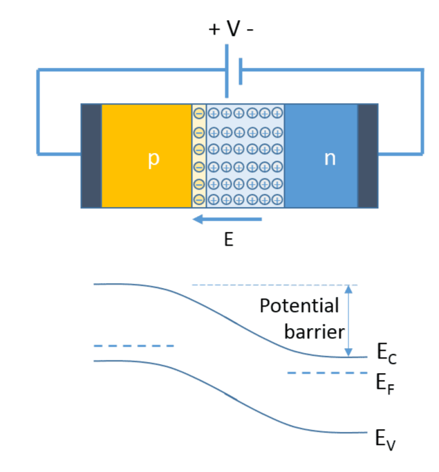
The p-n junction diode characteristics and operation are closely connected to the behavior of the carriers in the junction formed at the boundary between the p-type and n-type materials. The p-n junction is also the basic building block of a variety of other devices, and the basic techniques used for the analysis of the p-n junction can be extended to other problems. In this section, as our first simulation with the CHARGE solver, we study the basic characteristics of a silicon p-n junction diode. Specifically, we simulate the current-voltage curve and band structure of this device using the CHARGE solver.

Basic Workflow
In this video, we will show the typical workflow of the CHARGE simulation. The workflow is also commonly adopted by other Lumerical solvers in the Finite-Difference IDE environment.

