When to Use CHARGE — Lesson 2
As was mentioned in the previous unit, the CHARGE solver provides several simulation modes that can be used in many applications. In this unit, we briefly introduce some of these applications. Additional information, including simulation files, can be found in Lumerical’s Knowledge Base and also in the related links.
Electro-Optic Modulators
Electro-optic modulators, which encode an electrical signal on an optical carrier, have been the subject of a lot of interest, especially in the field of silicon photonics where on-chip light sources are not readily available and direct modulation of the source is often not practical. A variety of modulator designs have been proposed to try to overcome design requirements imposed by physical device size, power consumption, modulation depth, and bandwidth, including the Mach-Zehnder interferometer and modulator devices employing electro-absorption or resonant structures. As the performance requirements of these active components become more demanding, analysis and optimization of the modulator become a critical design task. Both optical and electrical simulations of modulators are necessary to fully characterize the device's performance in silicon photonics systems.
The CHARGE solver can be used to analyze the electrical characteristics of the modulators by defining the component geometry and doping profile and simulating the distribution of charge in the component in response to an applied voltage. Ansys Lumerical’s optical solvers, such as MODE or FDTD, can then be used to perform optical simulations of the guided-wave structures and extract the modulation response, such as phase and loss, as a function of the applied voltage.
Photodetectors
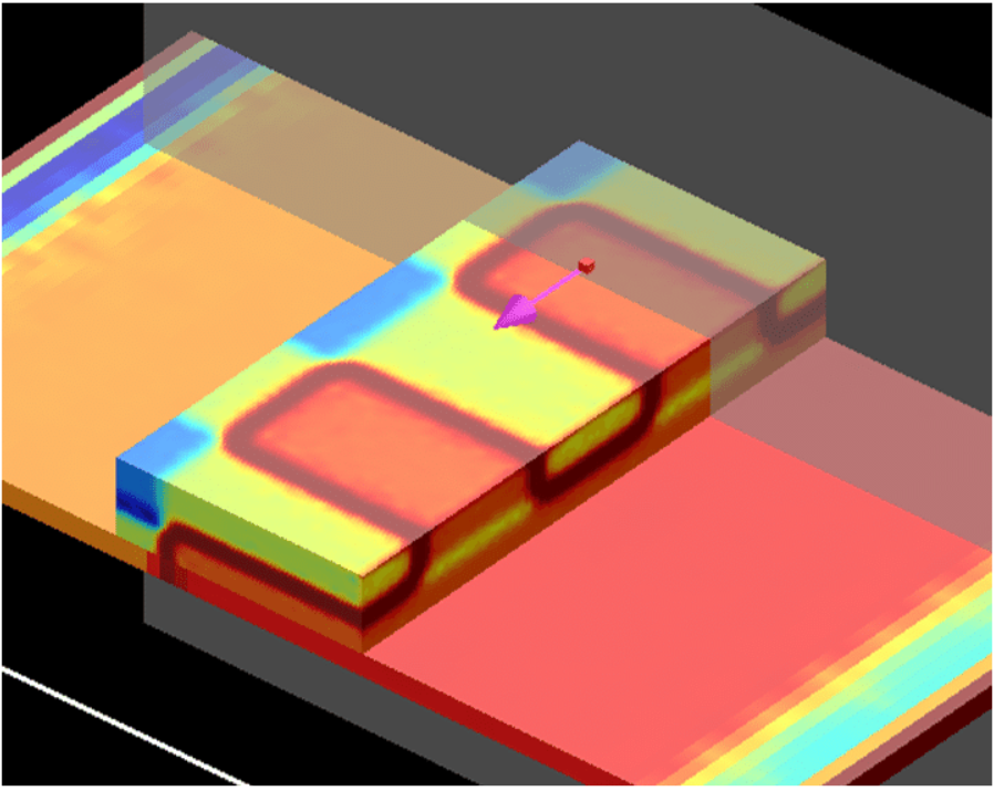
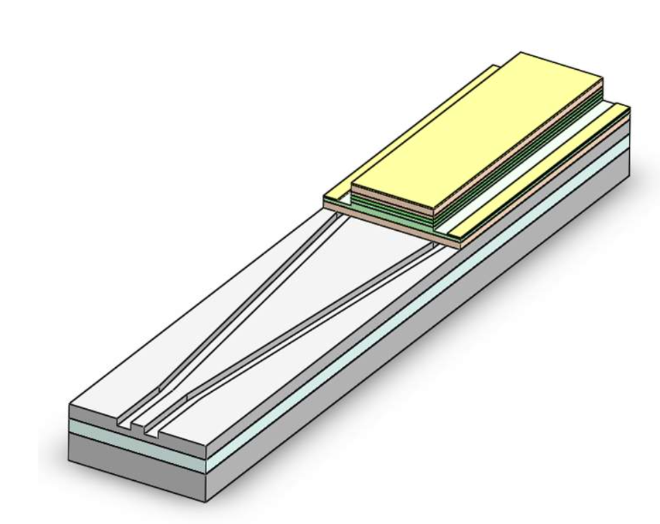
A photodetector, which converts an optical signal into an electrical signal, is a key component in any optical data communication link. When integrated into waveguides for on-chip communications, the photodetector requires a multiphysics electrical/optical analysis to accurately capture the effects of guiding light, photogeneration and current collection relevant to this type of device. Lumerical’s electrical and optical device solver products provide a powerful workbench for complete device simulation, yielding characteristics such as responsivity, dark current and detection bandwidth.
For the optical simulation, the FDTD can model in 3D the guiding of light into the active area of the device, absorption of the optical signal and the resulting generation of electrical charge. For electrical simulation, the CHARGE solver may be used to simulate the collection of the photo-generated charge within the active semiconductor region. The drift-diffusion method employed by CHARGE accurately models the transport of charge within the semiconductor device, accounting for a wide variety of physical effects.
CMOS image sensors
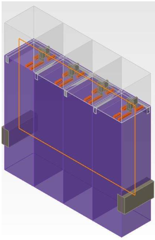
As CMOS image sensor pixels sizes shrink to pixel diameters of 1 micron and below, there has been continued research into overcoming technical challenges related to the production of images of sufficient quality, color depth, and resolution sufficient for demanding consumer and commercial applications. With the goal of producing CMOS imagers capable of capturing an incident light signal, and efficiently propagating that signal through sophisticated multilayer structures manufactured with CMOS fabrication processes, rigorous optical and electrical simulations that account for absorption, scattering, and diffraction from sub-wavelength features (like metallic interconnects for the readout electronics, or the curved dielectric surfaces of which the microlens array is constructed) as well as steady-state and transient electrical behavior of the sensor are required.
The FDTD is a high-performance optical solver that can be used to simulate the interaction of light with various components of a 3D CMOS pixel. The solver can be used to accurately and efficiently assess new design concepts, whether one is interested in analyzing the benefits of front-side versus backside illumination as it relates to light absorbed within the photodiode, optimizing the microlens shift for oblique angles of incidence, or exploring the impact of adding a light guide to the layer structure.
The spatial absorption calculated from FDTD can be converted into a generation rate for subsequent simulations in CHARGE solver to determine how much of the generated electrons can be collected and therefore the quantum efficiency of the device. CHARGE solver can account for the distribution of dopants that give rise to the built-in electric fields, the mobility of free carriers, and the physical processes that result in the recombination of charge.
Solar cells
With the goal of reducing manufacturing costs and material inputs and increasing solar cell efficiencies, research into solar cells is increasingly focused on new cell design concepts including thin film and textured-surface solar cells. When incorporating nanophotonic elements like metallic nanoparticles with plasmon resonances tuned to efficiently scatter the light into the absorbing layer, or nanotextured surface anti-reflection coatings to reduce undesirable back reflections that degrade cell performance, solar cell performance can be dramatically improved.
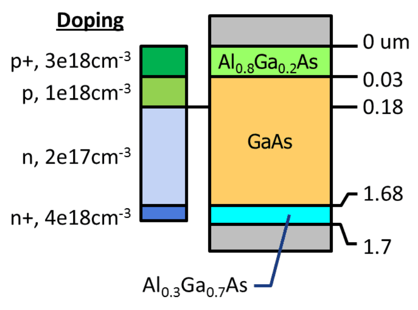
Simulation of solar cells is essential to predict the behavior of these devices. As the design of photovoltaic cells increases in complexity, it becomes more difficult to obtain analytic solutions to their performance. In the real device, non-ideal processes such as bulk and surface recombination of electrical charge carriers (electrons and holes) reduce the electrical efficiency of the solar cell. A combination of optical and electrical simulations that account for these non-ideal processes is necessary to accurately characterize the photovoltaic efficiency of the solar cell.
FDTD is a high-performance optical solver that can be used to simulate the interaction of light with a wide variety of solar cell designs. These designs can range from simple planar geometries to very complex patterning and can include a wide variety of materials such as organics and metals.
The result of the optical simulation is the spatial absorption in the substrate region, from which one can calculate the generation rate. This generation rate can be used in an electrical simulation in CHARGE to determine the responsivity and the photovoltaic efficiency of the solar cell. The CHARGE solver will account for the distribution of dopants that give rise to the built-in electric fields, the mobility of free carriers and the physical processes that result in the recombination of charge.
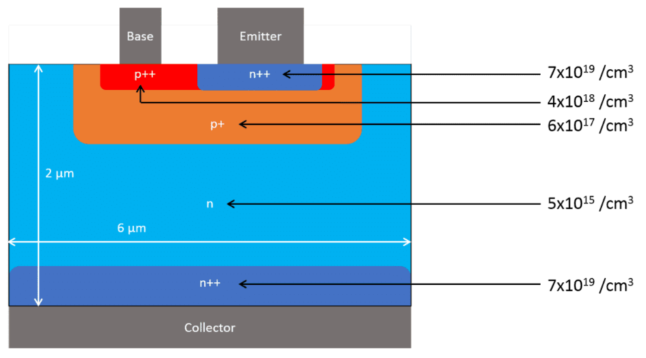
Electronic components
Electronic circuits consist of active components such as diodes, transistors, integrated circuits and passive components such as capacitors, resistors, etc. Today, most electronic devices use semiconductor components to perform electron control. The CHARGE solver is capable of modeling the steady-state and transient behavior of charge carriers in these semiconductor components.
