TAGGED: circuit, hfss, lumped-rlc
-
-
July 19, 2024 at 12:39 am
Stefano R
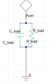
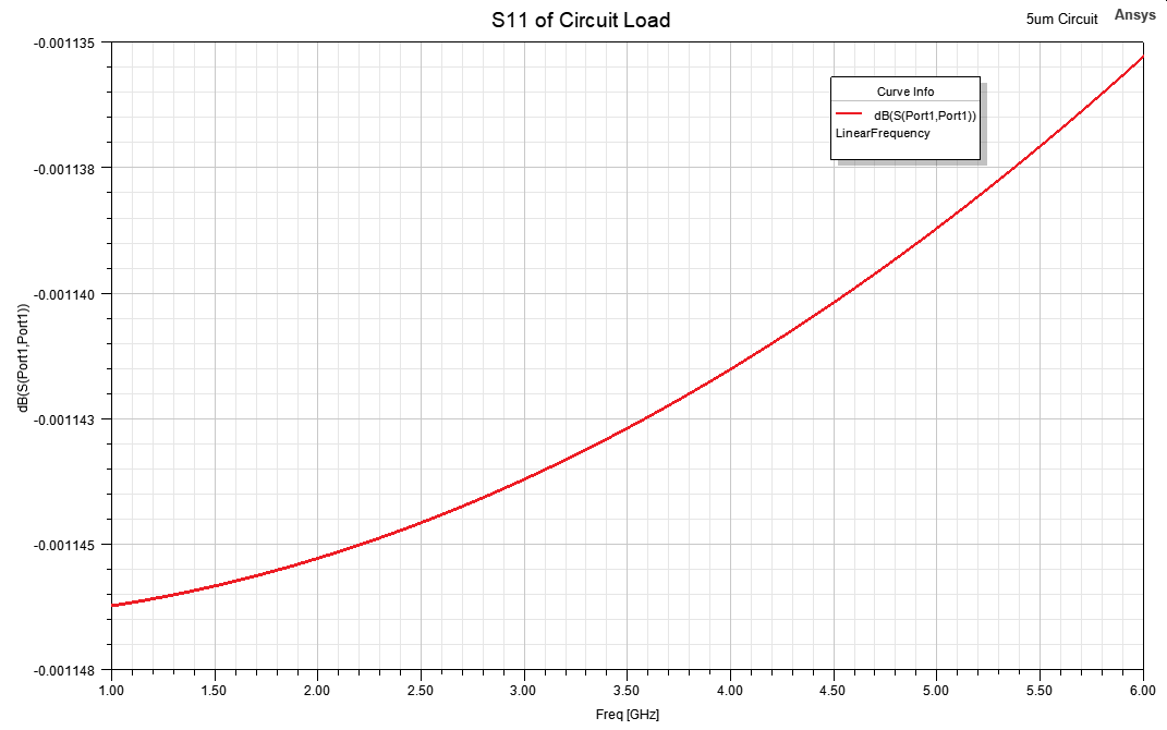
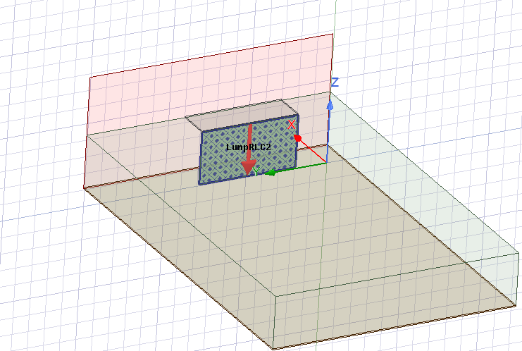
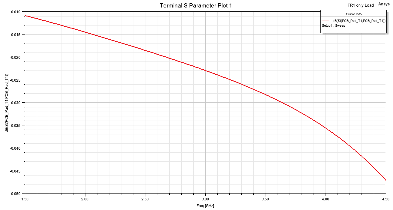
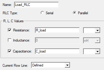
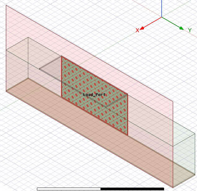
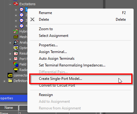
SubscriberThis is part of a larger project of simulating a PCB-fed resonator bonded to a lumped RLC load. I want to understand better the FEM model of the load versus the circuit representation. In the model, have a PCB microstrip wave port with Port_Z0 = 40. I want a parallel R and C (value R_load = 1MegaOhm and C_load = 40fF) shunted to the ground, as shown in the circuit diagram. Ground here is defined as the backplane of the PCB. What is the best way to connect the Lumped RLC component? These results differ from what I expected from the circuit representation. I know the S11 values are small here, but this is just a test to see if I can model the load well.
-
July 20, 2024 at 12:38 am
-
September 2, 2024 at 3:12 pm
-
Viewing 2 reply threads
- You must be logged in to reply to this topic.
Ansys Innovation Space


Trending discussions


- Polarization and Angle of Incidence Scan with Floquet ports in ANSYS HFSS
- How to create Lumped RLC in HFSS to match Circuit? (Simulate load as Lumped RLC)
- CPW resonant frequency HFSS Simulation
- EMA3D Current Source Problem
- Setting up CPW HFSS Simulation
- Simplorer link to Maxwell transient
- Help on calculating port impedance Zpv using Field calculator under HFSS please
- Question for Maxwell
- HFSS Incident Plane Wave excitement mode
Top Contributors


-
1086
-
447
-
396
-
225
-
201
Top Rated Tags


© 2024 Copyright ANSYS, Inc. All rights reserved.
Ansys does not support the usage of unauthorized Ansys software. Please visit www.ansys.com to obtain an official distribution.

